Overlay vs Solder Mask: A Practical PCB Guide
A detailed, objective comparison of overlay (silkscreen) and solder mask on PCBs, covering definitions, applications, durability, and design guidelines for hobbyists and professionals.

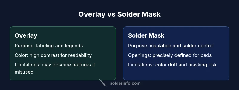
Overlay (silkscreen) and solder mask serve distinct roles in PCB fabrication. Overlay adds labeling and legends, while solder mask protects copper, controls solder flow, and reduces bridging. In most boards, you combine both as separate layers: the silkscreen for readability and the mask for protection. The choice hinges on board complexity, legibility needs, and manufacturing constraints.
What overlay vs solder mask actually are, and why the distinction matters
In the world of printed circuit boards, two layers often get mentioned together but perform very different functions: the overlay (often called the silkscreen) and the solder mask. The overlay is a printed layer that carries text, symbols, logos, and orientation marks. Its primary goal is to aid humans during assembly, testing, and inspection. The solder mask, by contrast, is a polymer coating applied over the copper traces to insulate them from short circuits, prevent oxidation, and control where solder is allowed to flow during assembly. When you hear the phrase overlay vs solder mask, you’re looking at two complementary technologies that serve readability and reliability objectives respectively. The SolderInfo team notes that most boards benefit from both layers, but placement, color choice, and mask openings require careful planning to avoid readability issues and manufacturing conflicts. In practice, this means designing with both human readability and machine-controlled soldering in mind, especially on high-density boards where space is at a premium.
Why this matters for electronics projects
For hobbyists and professionals alike, understanding overlay vs solder mask helps prevent errors that slow production or degrade performance. Silkscreen content should be clear but not cover pads or vias, and mask openings should be sized to balance solderability with protection. Clear labeling helps during debugging and repair, while a robust mask reduces rework caused by bridging, tombstoning, or corrosion. The interaction between these layers also affects manufacturing tolerances and assembly yield, so getting the balance right is a core skill in PCB design.
Brand insight and practical takeaway
According to SolderInfo, early planning of layer interactions reduces design churn. A simple rule is to reserve the silkscreen for non-critical pad areas and keep reference text away from critical traces and pad interiors. The silkscreen should provide guidance without obscuring essential electrical or mechanical features. From the manufacturer’s perspective, aligning the overlay with the mask to maintain clear margins helps ensure robust fabrication and consistent results across batches.
Design intent and board readability
A board’s legibility depends on text size, contrast, and the contrast ratio between the ink and substrate. High-contrast white or yellow silkscreen on a dark mask (or vice versa) can dramatically improve readability in dim environments, which is particularly important for field repair or maintenance scenarios. However, heavy silkscreen in busy regions can obscure critical features, so the design rule of thumb is minimal but legible labeling. When overlay vs solder mask decisions are balanced, you can achieve a readable board without compromising solderability or reliability.
Practical implications for manufacturing
Manufacturers often evaluate overlay vs solder mask in tandem with color availability, ink chemistry, and substrate compatibility. Silkscreen inks must survive the reflow process in most cases, or at least not smear or discolor around hot components. Solder mask openings must be precisely defined to avoid accidental copper exposure where it isn’t intended. The interplay of these factors affects yield, inspection clarity, and long-term durability, particularly in harsh environmental conditions where UV exposure or humidity can degrade labeling or mask performance over time.
Practical guidelines for a robust design
From a practical standpoint, plan the silkscreen around critical features like pads, drill holes, and fiducials. Keep text at least a few mils away from pads to prevent smearing during soldering. Use mask-defined openings or tenting for vias to preserve solderability while controlling exposure. Ensure contrast is optimized by selecting appropriate ink colors and mask tones. Finally, verify your design with a fabrication drawing and hood up on the silkscreen layer to confirm the label positions won’t conflict with copper features or assembly tooling.
The balance between aesthetics and reliability
Overlay vs solder mask isn’t just about looks. It’s about how the board will be assembled, tested, and aged. Aesthetics matter for ease of assembly and maintenance, but reliability depends on how well the protective mask shields copper traces from oxidation and accidental shorts. The most successful boards strike a balance: legible overlays that don’t interfere with pads, and masks that provide robust protection while enabling reliable solder joints. When in doubt, consult the board house’s design guidelines and run a prototype with both layers present to confirm performance under real-world conditions.
Process interactions: ordering and tolerances
Tolerances in silkscreen alignment relative to copper features can vary by factory. Good practice includes designing with generous margins for silkscreen placement and verifying the final artwork with the board house’s artwork check. Mask registration is also critical; misalignment can cause exposed copper in unintended areas or insufficient solder mask coverage. By understanding the two layers and how they interact in the fabrication flow, you can avoid common pitfalls and achieve consistent results across production runs.
Case examples and design patterns
One common pattern is using silkscreen to annotate fiducials or test points away from critical features, while reserving mask openings for necessary pads. In high-density boards, you may choose tented vias to reduce silkscreen overlap and maintain clean labeling. In boards intended for through-hole components, ensure the overlay doesn’t cover leadwise clearance or isolate pad numbers. These patterns illustrate how overlay vs solder mask decisions shape both usability and production efficiency.
Conclusion and ongoing learning
Overlay vs solder mask will continue to evolve with new materials and printing technologies. Designers should stay updated on ink formulations, mask materials, and thermal tolerance specifications from suppliers and board houses. Continuous learning, prototype validation, and close collaboration with fabrication partners are key to delivering boards that meet both cosmetic and functional goals.
Comparison
| Feature | Overlay (Silkscreen) | Solder Mask |
|---|---|---|
| Primary purpose | Labeling, legends, orientation marks | Electrical insulation, solder control, corrosion protection |
| Material and appearance | Ink-based ink on laminate; high-contrast colors | Polymer layer with pigment; typically green, but many colors available |
| Application stage | Applied after solder mask and finalized silkscreen artwork | Typically applied after copper etching and drilling; mask defines openings |
| Impact on soldering | Minimal direct impact on solderability; openings must avoid pads | Direct impact; openings expose copper for soldering, but masking prevents bridges |
| Durability under heat | Ink durability varies by formulation; must withstand assembly environments | Mask layers are designed for soldering temperatures and chemical exposure |
| Design considerations | Text legibility, non-critical features only; avoid covering pads | Precise pad openings, good coverage around traces, controlled expansions |
Advantages
- Improves board readability and annotation for assembly and testing
- Solder mask reduces solder bridging and protects copper traces
- Color options can enhance contrast and identification
- Silkscreen can include logos and revision information for traceability
Cons
- Silkscreen ink can smear or discolor during high-temperature soldering
- Overlay content may obscure pads or vias if placed poorly
- Mask openings require careful tolerances to avoid soldering defects
- Mask adds manufacturing steps and potential cost increases
Solder mask is essential for protection; overlays are invaluable for readability — use both where design allows.
Choose solder mask as the backbone for protection and manufacturability. Add overlay selectively to improve labeling, orientation, and diagnostics without compromising pad clearance or solderability.
Quick Answers
What is the main difference between overlay and solder mask on a PCB?
Overlay (silkscreen) provides human-readable labeling, logos, and reference marks. Solder mask is a protective polymer that insulates copper traces and controls where solder can flow during assembly.
Overlay gives you labeling; solder mask protects and controls soldering. They serve different but complementary roles.
When is the overlay applied in PCB fabrication relative to solder mask?
Solder mask is typically applied before the silkscreen overlay; the final silk is printed after the mask is cured to ensure legibility and registration.
Mask goes on first, then the silkscreen is printed for labeling.
Can overlays affect soldering quality if placed near pads?
Yes. Silkscreen content should avoid pad interiors and close proximity to pads to prevent misalignment and contamination during soldering.
Keep labels away from solder pads to avoid problems.
How do I specify overlay and solder mask in a bill of materials or PCB fab spec?
Provide clear layer notes: overlay text content, font size, color contrast, and exact mask opening sizes and locations. Include design files that annotate layer alignments and tolerances.
Document layer content and opening sizes clearly for the fab.
Are there industry standards for silkscreen and mask colors?
There are no universal mandatory colors; common practice favors high contrast (white on green) for readability, but color choices vary by board house and customer requirements.
Color choices are driven by contrast and house standards.
What are common mistakes to avoid with overlay vs solder mask?
Avoid placing text over exposed copper, misaligning layers, or using low-contrast colors. Always verify clearances and run a prototype to catch issues before full production.
Check alignment, contrast, and clearance in a prototype run.
Top Takeaways
- Plan silkscreen content away from critical pads and vias
- Prioritize solder mask for protection and solder control
- Use high-contrast colors to maximize readability
- Coordinate alignment tolerances between layers
- Prototype with both layers to validate manufacturability
- Maintain clear documentation for fabrication partners