Solder Resist vs Solder Mask: A Practical Side-by-Side Guide
Explore solder resist vs solder mask, their purposes, applications, and how to choose the right coating for PCB fabrication, electronics projects, jewelry soldering, and plumbing work.

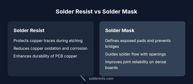
Solder resist and solder mask are protective coatings used during soldering and PCB fabrication, but they serve different roles. Solder resist primarily shields copper traces on PCBs from oxidation and etching, while solder mask governs where solder can flow, exposing pads and protecting nearby copper. For most hobby electronics and professional boards, the mask is critical for fine-feature reliability, while resist is essential for long-term PCB durability.
What solder resist and solder mask are, in plain terms
Solder resist and solder mask are protective coatings applied during PCB fabrication and soldering processes. In the realm of electronics manufacturing, a solder mask is the film that sits over copper traces but leaves holes for pads and vias; it acts as a barrier to prevent solder bridges in crowded boards. Solder resist, while often used interchangeably with solder mask in common speech, can refer more broadly to the protective coating concept that guards copper during etching and handling. In many contexts, the terms overlap, but the practical distinction lies in exposure control and the stage of manufacturing. According to SolderInfo, understanding these coatings begins with recognizing that masking strategies influence yield, reliability, and manufacturability. For jewelry and plumbing, these concepts translate to protective layers that limit solder flow and protect underlying metal during heat cycles. In short, resist protects; mask guides soldering.
Core differences: scope, materials, and surface exposure
The primary difference between solder resist and solder mask is scope. Solder resist is the protective layer applied to copper before etching and general PCB processing, preventing unwanted reactions and corrosion on exposed copper during handling. Solder mask, on the other hand, is the patterned coating that defines exposed pads and keeps solder away from trace regions, guiding where solder will bond. Materials are both polymer-based epoxy or acrylic formulations, but masks tend to be formulated for precise openings and robust adhesion through multiple thermal cycles. The result is a balance between protection and solderability. In practice, resist coverage emphasizes board-level durability, while mask coverage emphasizes solder joint quality and feature accuracy.
Application contexts: PCB fabrication vs jewelry and plumbing
PCB fabrication relies on solder resist/mask to control solder flow and protect copper features across the board. Modern, photoimageable masks enable fine-feature traces and tight vias, supporting high-density interconnects. Jewelry and plumbing soldering use resist-like coatings to prevent unintended solder bonding and to shield areas not meant to be joined. In these contexts, the coating often serves as a temporary barrier during heat exposure, then is removed or left as a protective layer depending on the process. The key takeaway is that, regardless of industry, the coating must withstand heat, flux exposure, and cleaning solvents without cracking or delaminating. The SolderInfo approach emphasizes matching coating properties to the substrate and soldering method for best results.
Optical clarity, thickness, and coverage: how much mask/resist and tolerances matter
Coating thickness and coverage directly affect solderability and feature accuracy. Masks require precise thickness to avoid bridging or dampened pad exposure, while resist must maintain uniform thickness to protect traces without inflating trace widths. Any irregularity in opening size or mask clearance can lead to reduced solder fillet control or short circuits. In high-density boards, tolerances become critical; a slight misalignment can expose unintended copper or obscure a pad. For jewelry or plumbing, consistent coverage prevents unwanted solder spread and keeps joints strong. A consistent, manufacturer-approved process minimizes defects and accelerates soldering.
Practical guidelines for electronics hobbyists
For DIY electronics, choose solder mask for reliable pad exposure and to reduce accidental shorting on hobby PCBs. Ensure your thickness and cure profiles align with your substrate and soldering method (reflow vs hand-soldered). When reworking, masked areas require careful removal steps to avoid residue or delamination. Keep openings clean and aligned with pad footprints to avoid solder bridging. SolderInfo recommends coordinating mask design with footprint libraries and ensuring artwork for openings is validated before fabrication.
Practical guidelines for jewelry and plumbing soldering
In jewelry soldering, a resist-like barrier helps manage solder flow and protects delicate parts from overheating. For plumbing, protective layers can reduce oxidation and improve alloy compatibility during heat cycles, though different standards apply. Always select coatings that withstand your specific alloys and fluxes, and plan for post-solder cleaning to remove any residue. Consider the removal method: some coatings are sacrificial and easily peeled, while others require chemical strippers compatible with your substrate. The goal is clean joints, minimal cleanup, and minimal damage to surrounding material.
Common failure modes and troubleshooting tips
Common issues include pinholes, delamination, or edge lift in the mask, and insufficient protection or over-exposure with resist. Warping or peel-back often results from improper curing or substrate mismatch. Remedies include validating cure profiles, verifying exposure patterns, and selecting a masking solution compatible with your flux and solder alloy. Regular test coupons help monitor adhesion and reflow performance. SolderInfo highlights the importance of simulating your real-world conditions (temperature cycles, humidity, and cleaning solvents) to anticipate failures.
When to choose solder resist vs solder mask in mixed projects
In mixed projects, evaluate the dominant requirement: number of exposed pads, trace density, and the need to prevent solder bridging. For high-density electronics, mask is typically essential. For boards or assemblies subject to aggressive environments or repeated rework, resist may add value by enhancing copper durability. If you anticipate future rework or cleaning steps, plan mask openings to allow easy access and repeated soldering. The decision should balance manufacturability, reliability, and cost.
Future trends and evolving materials
Advances in photoimageable resists and low-temperature mask materials promise better adhesion, thinner profiles, and improved thermal stability. Expect masks with longer shelf life, easier removal in redevelopment, and compatibility with lead-free solder chemistries. As the industry trends toward finer pitches and flexible substrates, coating formulations continue to evolve to reduce defects and simplify processing. SolderInfo expects ongoing improvements in alignment tolerances, environmental resistance, and processing simplicity for both resist and mask technologies.
Comparison
| Feature | Solder resist | Solder mask |
|---|---|---|
| Primary purpose | Protect copper traces during etching and handling | Define exposed pads and protect solder joints during soldering |
| Typical substrate | Printed circuit boards (copper traces on FR-4 or similar substrates) | PCB boards and other substrates requiring controlled solder flow |
| Application method | Applied as a protective layer before etching; may be patterned for openings | Patterned layer that exposes pads and vias; applied to control solder flow |
| Material considerations | Epoxy- or acrylic-based protective coating; designed for etching resistance | Polymer-based, photoimageable or screen-printed coating with precise openings |
| Thermal and chemical tolerance | High resistance to etchants and ambient moisture; thermally stable during handling | Withstands soldering heat and flux exposure; must tolerate rework temperatures |
| Impact on manufacturability | Adds protection and durability; requires alignment with PCB design | Critical for defining solderable area; directly influences joint quality |
| Best for | Board durability, long-term copper protection | Precise solder joint definition on high-density or mixed-technology boards |
Advantages
- Reduces solder bridging by controlling exposure areas
- Protects copper traces from oxidation and chemical attack
- Improves process control and manufacturing yields
- Provides insulation and environmental protection for boards
- Widely supported in PCB fabrication workflows
Cons
- Requires precise application and alignment; adds process steps
- Improper curing or misalignment can cause defects
- Mask thickness can slightly alter pad geometry and solderability
- Temporary or sacrificial coatings may require removal steps in rework
Solder resist is essential for PCB durability and copper protection, while solder mask is critical for reliable solder joints and high-density layouts.
For PCB projects with dense traces, prioritize solder mask to prevent bridging and ensure pad exposure. Use solder resist to protect copper through manufacturing. In mixed scenarios, plan mask openings carefully and validate with test coupons to minimize failures.
Quick Answers
What is the difference between solder resist and solder mask?
Solder resist is a protective coating applied to copper traces to prevent oxidation and etching damage, while solder mask defines exposed pads and controls solder flow during assembly. In practice, masks are patterned to allow solderability, whereas resist focuses on copper durability.
Solder resist protects copper traces; solder mask shapes where solder can go. Remember, mask openings expose pads for soldering.
Where is solder mask typically used?
Solder mask is used on PCBs to prevent solder bridging between traces, especially in high-density boards. It’s patterned to expose pads and vias, ensuring reliable solder joints and manufacturability.
Mask is used on PCBs to keep solder where it should be and protect the rest of the copper.
Can resist be used in jewelry or plumbing soldering?
Yes, similar coating concepts apply in jewelry and plumbing to control solder flow and protect surrounding metal. Always choose a coating compatible with the alloy and heat cycle used in those domains.
Coatings help control solder spread in jewelry and plumbing, just like on PCBs.
How do I remove damaged mask or resist after soldering?
Removal depends on the coating type and substrate. Use manufacturer-approved solvents or mechanical methods that won’t damage the substrate. Always test on a small coupon before large-scale removal.
Follow the coating’s removal steps from the data sheet and test first on a sample.
What factors influence coating choice for hobby projects?
Consider pad density, expected rework, environmental exposure, and your fabrication method. For dense boards, mask is critical; for durability of copper, resist adds protection.
Density, rework needs, and environment guide your coating choice.
Top Takeaways
- Protect copper traces with the appropriate resist or mask
- Mask openings govern where solder can flow and where joints form
- Choose coatings based on board density, exposure, and future rework
- Validate processing with samples and test coupons