Paste Mask vs Solder Mask: An Analytical Guide for PCB Fabrication
Analytical comparison of paste mask and solder mask for PCB fabrication, covering definitions, deposition processes, interactions, and best-practice guidelines for designers and assembly technicians.

Paste mask vs solder mask are two distinct PCB mask layers that serve different roles in fabrication. Paste mask defines where solder paste is deposited for component placement, while solder mask protects copper features and prevents bridging during soldering. The right choice depends on the board's complexity, stencil tolerance, and assembly method.
Paste mask vs solder mask: scope and definitions
Paste mask vs solder mask represent two masked layers that govern distinct steps in printed circuit board manufacturing. According to SolderInfo, the paste mask defines where solder paste is deposited on component pads, while the solder mask protects copper traces from oxidation, prevents solder bridging, and defines where copper is exposed for soldering. The distinction matters for yield, reliability, and manufacturability, particularly on boards with fine-pitch components, complex copper geometry, or mixed-technology assembly. Designers must consider paste mask precision, stencil tolerances, and reflow profiles in tandem with solder mask coverage to achieve consistent joints. The goal is to minimize rework and ensure robust assembly across varying production environments, from hobbyist prototyping to high-volume manufacturing.
Paste mask: definition, materials, and application
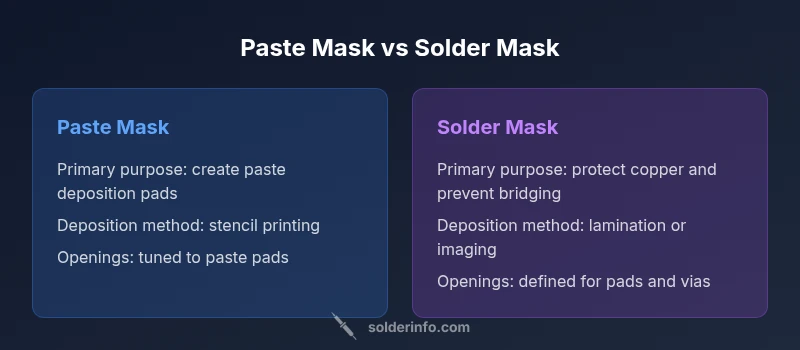
A paste mask, often realized as a solder paste stencil, is a patterned sheet that sits above the PCB during stencil printing. Openings align with solderable pads and vias to control where paste is deposited. Materials commonly used for paste masks include stainless steel, nickel, and polymer composites, chosen for durability and manufacturability. The stencil thickness and aperture geometry influence paste volume and print consistency, which in turn affect solder fillet formation during reflow. For hobbyists and professionals, the paste mask workflow is tightly integrated with the stencil printer, paste formulation, and component placement accuracy. When designed properly, paste masks enable repeatable prints across multiple boards and minimizes paste smearing or smearing-based bridging.
Solder mask: definition, materials, and application
Solder mask, also known as solder mask or solder resist, is a protective layer applied to copper traces to prevent oxidation and to reduce unintended solder bridging. It can be applied via liquid photoimageable (LPI) processes, screen printing, or dry film lamination. The mask typically defines openings where copper pads or exposed copper will be soldered, while the rest of the board remains insulated. Materials for solder mask are designed for chemical resistance and adhesion, and the layer’s thickness is chosen to balance protection with thermal tolerance during soldering. In practice, solder mask affects both manufacturability and reliability by controlling where heat is applied and how easily pads can be reworked if necessary.
Mask interaction during assembly: alignment and registration
During assembly, paste mask and solder mask work in concert with the board layout. Proper alignment (registration) ensures that paste openings land exactly on pad surfaces and that solder mask openings align with copper features. Misregistration can cause poor printing, open circuits, or bridged joints. The deposition path for paste relies on precise stencil alignment with the PCB, while solder mask relies on accurate panelization and imaging steps to keep openings aligned with pads and vias. In high-density boards, even small misalignment can propagate defects across multiple components. Quality control measures—such as optical inspection after printing and post-lamination mask checks—help detect misregistration early in the process.
Key differences in deposition, tolerance, and defect profiles
The paste mask governs solder paste deposition and is therefore tightly coupled with stencil print quality, paste viscosity, and reflow profile. Its defects typically include incomplete paste transfer, smearing, or non-uniform volumes that lead to insufficient solder or tombstoning on small components. The solder mask mainly affects surface insulation and pad exposure; defects include lifted mask edges, insufficient openings, or mask slivers that can trap residues. Tolerances differ: paste mask errors often relate to volume and alignment in the stencil area, while solder mask issues more commonly concern edge coverage and opening geometry. Understanding these defect profiles helps teams implement targeted inspection steps and process controls.
Design implications: layout considerations for paste mask and solder mask
Effective design for paste mask and solder mask requires planning pad spacing, paste aperture sizing, and solder-mask openings in harmony with component packages, stencil capabilities, and soldering methods. For fine-pitch parts, both masks demand tighter control: paste volumes must be predictable, and mask openings must avoid collapse of paste or leakage. Designers should consider the solder mask clearance around pads, via tenting when needed, and the presence of copper features near edges that could cause bridging. Clear documentation for fab houses, including masked layer drawings and aperture list, reduces ambiguity and improves yield.
Manufacturing implications: cost, lead times, and reliability
Mask layers influence fabrication cost, lead time, and long-term reliability. Paste mask may introduce additional stencil production steps, which can impact turnaround times, while solder mask adds an additional lamination or imaging step. Reliability considerations include mask adhesion, environmental exposure, and thermal cycling tolerance. When boards feature mixed-technology assembly (e.g., surface-mmount devices with through-hole components), the combined mask strategy must be validated through prototypes and test coupons. Transparency with the fabricator about tolerances, paste volume targets, and solder-mask coverage is essential for predictable results across runs.
Practical guidelines for choosing mask strategy across projects
The choice between paste mask and solder mask decisions should be driven by the assembly method and the board’s function. For boards relying on precise paste deposition (e.g., fine-pitch LEDs or select components), prioritize paste mask accuracy and stencil quality, and align with paste formulation and printing cadence. For boards with mixed copper features or high-density routing, ensure robust solder-mask coverage to prevent bridging and oxidation and to preserve corrosion resistance. In many cases, a hybrid approach—careful paste mask design complemented by a well-defined solder mask—yields the most reliable results. Always run a pilot panel to validate print, inspect, and reflow outcomes before committing to production.
Case considerations for mixed-mask boards: when to use each type
In complex boards featuring both high-density SMT regions and high-reliability requirements (such as aerospace or medical devices), a combined mask strategy is common. Paste mask is used where paste deposition must be controlled with excellent repeatability, while solder mask provides robust protection across exposed copper and non-solderable regions. Designers should map paste deposition zones to pad arrays and ensure mask openings do not intersect with test coupons or fiducials. Clear communication with the PCB fabricator about stack-up, lamination order, and imaging steps helps minimize variability and ensures consistent results across multiple production lots.
Common mistakes and troubleshooting tips
Common mistakes include underestimating paste volume, misinterpreting stencil apertures, or misaligning mask layers to the board. Troubleshooting starts with a robust inspection plan: verify paste volume and alignment after stencil printing, confirm solder-mask opening integrity under optical inspection, and run test reflow profiles to detect bridging or insufficient vias exposure. If defects occur consistently in a region, recheck aperture geometry, plating quality, and alignment marks. Document any mask-related defects and adjust CAM data or fabrication notes accordingly to prevent recurrence.
The role of paste mask vs solder mask in advanced applications
In advanced applications—such as boards with high reliability requirements, fine-pitch components, or mixed-assembly technologies—the paste mask and solder mask strategy becomes a design and fabrication discipline. This discipline includes precise CAM data, standardized mask library definitions, and rigorous process controls. It often involves close collaboration with the fabricator to tailor mask thickness, aperture tolerance, and post-print cleaning to meet performance specifications. The end goal remains straightforward: accurate deposition where needed and robust protection where necessary to ensure consistent, high-yield production.
Comparison
| Feature | Paste mask (paste mask layer) | Solder mask |
|---|---|---|
| Primary purpose | Governs solder paste deposition for component placement | Protects copper traces and defines solderable areas |
| Deposition/application method | Stencil-driven paste deposition with openings aligned to pads | Laminate or image-based mask with openings aligned to pads and traces |
| Material considerations | Stencil material (stainless steel, nickel, or polymer) designed for paste printing | Mask material chosen for adhesion and chemical resistance |
| Tolerance and alignment | Paste print tolerances depend on stencil quality and printer alignment | Mask alignment governs exposure accuracy and edge definitions |
| Impact on defects | Paste-related defects include insufficient or excessive paste and smearing | Mask-related defects include bridging, lifted edges, or masked areas |
| Cost and lead time | Paste mask adds stencil production steps and potential print variability | Solder mask adds lamination/imaging steps and generally increases protection |
Advantages
- Enables precise solder paste deposition for reliable joints
- Enhances copper protection and solder joint integrity
- Supports complex board layouts with varied component types
- Established workflows and compatibility with standard PCB processes
Cons
- Adds stencil production and potential alignment risk
- Requires tight process controls for paste volume and placement
- Mask defects can impact rework and yield if not detected early
Both masks are essential; use paste mask for controlled paste deposition and solder mask for copper protection and defined solderable areas.
A well-planned combination minimizes defects and maximizes yield. Prioritize alignment, aperture accuracy, and process controls to ensure robust fabrication across production runs.
Quick Answers
What is paste mask used for in PCB manufacturing?
A paste mask defines where solder paste is deposited on pads during stencil printing. It ensures accurate paste volume and placement, which directly affects solder joint quality after reflow.
A paste mask controls where solder paste is laid down on pads, ensuring the right amount of solder for each component.
How does solder mask protect copper and prevent solder bridges?
Solder mask covers most copper areas except the pads and vias, protecting against oxidation and preventing unintended solder bridges between adjacent pads during reflow.
Solder mask shields copper traces and prevents bridges during soldering.
Can paste mask be used without solder mask?
Yes, some boards print paste on selected regions without a full solder mask. However, leaving copper exposed increases risk of oxidation and bridging unless other protections are in place.
It’s possible to use paste mask alone, but it raises oxidation and bridging risks if copper isn’t protected elsewhere.
What materials are used for paste mask and solder mask?
Paste masks use stencil materials such as stainless steel or polymer with defined openings; solder masks use photoimageable or laminated materials designed for adhesion and chemical resistance.
Paste masks use durable stencils, while solder masks use adhesive, chemical-resistant membranes.
What are common mistakes when designing mask openings?
Common errors include misaligned apertures, incorrect pad clearances, and openings that are too large or too small for the intended solder paste or soldering heat. Thorough CAM review and prototype testing help prevent these issues.
Misaligned or poorly sized openings are frequent mask mistakes; prototype testing helps catch them.
Top Takeaways
- Define mask roles early in the design phase
- Ensure precise alignment between paste openings and pads
- Use solder mask to prevent bridging on exposed copper
- Prototype with a pilot run to validate mask performance
- Coordinate with the fabricator on tolerances and CAM data