Solder Mask vs Silkscreen: A Practical PCB Guide
Explore solder mask vs silkscreen on PCBs, their distinct roles, application methods, color options, and how to design for manufacturability. A balanced, analytical look for DIYers and professionals.

According to SolderInfo, solder mask and silkscreen serve distinct, essential roles on a PCB. The solder mask protects copper traces and controls solder flow, while silkscreen provides assembly labels and design notes. In practice, using both thoughtfully improves reliability, manufacturability, and serviceability. This comparison will help you decide when to emphasize one layer over the other in your board design.
Solder mask vs silkscreen: Definitions and core roles
In PCB design, solder mask (often called solder resist) and silkscreen occupy different physical layers and fulfill different purposes. Solder mask is a protective polymer layer that covers copper traces to prevent accidental solder bridges, protect circuitry from oxidation, and guide soldering for pads and vias. Silkscreen is ink printed on top of the mask to convey information such as component designators, reference marks, and simple assembly notes. Understanding solder mask vs silkscreen is crucial because each layer shapes how readable a board is, how reliably it can be manufactured, and how easy it is to troubleshoot later. For hobbyists and professionals alike, a thoughtful balance between these two layers reduces rework and improves serviceability. The SolderInfo perspective emphasizes practical decisions that align with board density, intended use, and the manufacturing workflow.
Key takeaway: Solder mask handles electrical safety and manufacturability, while silkscreen enhances human readability and documentation. This distinction guides where to invest design effort and budget in your PCB project.
Comparison
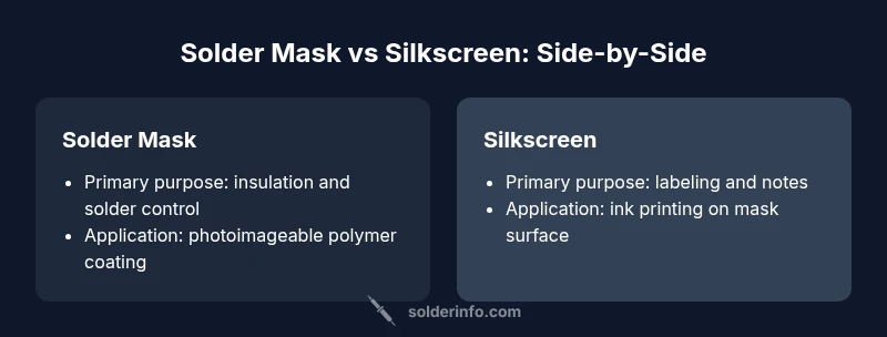
| Feature | Solder mask | Silkscreen |
|---|---|---|
| Primary purpose | Insulates copper traces, controls solder flow, and protects exposed copper | Labels components, references, and notes on the board surface |
| Application method | Photoimageable polymer coating applied during fabrication and cured | Ink-based printing (screen or pad) on the PCB surface, usually after masking |
| Impact on assembly | Critical for electrical reliability; misalignment or overexposure can create defects | Aids assembly operators by identifying parts; does not affect electrical function |
| Color and visibility | Commonly green by default, with other colors available; translucency varies | Typically white or light-colored ink; visibility depends on board color and lighting |
| Cost and manufacturability | An essential fabrication step that affects yield and defect rates | Adds some material and printing steps, but is generally a modest cost for readability |
Advantages
- Solder mask reduces solder bridges and shorts on dense traces
- Mask improves long-term reliability by protecting copper
- Silkscreen enhances human readability during assembly and repair
- Color customization can improve traceability and documentation
- Coordinated use of both layers supports better fault diagnosis
Cons
- Silkscreen near pads can obscure solderability if misapplied
- Excessive ink or improper mask openings can complicate rework
- Dense boards may require silkscreen reduction to avoid crowding pads
- Color choices for masks and silkscreen ink can add complexity and cost
Prioritize solder mask for electrical reliability; use silkscreen selectively for clarity.
Solder mask is essential for protecting copper and ensuring clean solder joints, especially in high-density layouts. Silkscreen adds valuable assembly notes but should be applied with care to avoid obscuring critical pads. The best boards balance both layers, applying mask comprehensively while silkscreen is reserved for non-critical areas.
Quick Answers
What is the primary purpose of solder mask on a PCB?
The primary purpose of solder mask is to insulate copper traces, prevent solder bridges during assembly, and protect exposed copper from oxidation. It also helps control where solder is allowed to flow, which is crucial for reliable solder joints. This layer is essential for functional boards, especially in dense or high-pin-count designs.
Solder mask insulates copper and prevents solder bridges, which keeps your board reliable during assembly.
How does silkscreen differ from solder mask in function?
Silkscreen serves as a documentation layer, printing component designators, outlines, and notes directly onto the board. It does not affect electrical performance but greatly aids assembly, troubleshooting, and future maintenance. The two layers complement each other, with mask handling electrical aspects and silkscreen enhancing human readability.
Silkscreen labels parts and notes, helping humans read the board without changing its electrical behavior.
Can silkscreen affect soldering quality?
Yes, if silkscreen ink encroaches on exposed pads or vias, it can interfere with solder wetting and joint formation. Modern boards avoid printing over pads, and if silkscreen is used near pads, it should be kept clear of the solderable area. This is a common point of caution for designers.
Ink on pads can hinder soldering, so silkscreen is kept away from exposed copper areas.
Should I omit silkscreen near SMD pads?
Yes, silkscreen near SMD pads is often omitted or minimized to prevent interference with soldering and DPIs (density of information). For dense or fine-pine components, silkscreen is selectively applied in non-critical zones. This practice helps maintain solderability and yields.
Avoid printing directly on SMD pads to prevent soldering issues.
What factors influence color choices for solder mask and silkscreen?
Color is chosen to optimize readability, contrast, and maintenance needs. Green remains common for mask due to legacy and visibility, while silkscreen ink is typically white or light colors for contrast. Consider environmental factors, such as lighting and glare, and plan for future inspections when selecting colors.
Choose mask colors with good contrast to the silkscreen and make sure labels stay readable.
Are there industry standards governing mask and silkscreen?
Standards-related guidance for solder mask and silkscreen typically comes from IPC guidelines and industry best practices rather than a single universal standard. These guidelines address clearances, pad openings, and labeling conventions to ensure manufacturability and reliability.
IPC guidelines provide best-practice recommendations for mask and silkscreen layouts.
Top Takeaways
- Prioritize solder mask for electrical isolation and soldering reliability
- Use silkscreen to label components and provide assembly notes
- Coordinate mask openings with pad geometries to avoid manufacturing issues
- Avoid dense silkscreen near exposed copper to prevent soldering defects
- Plan color choices early for readability and durability