Solder Mask Defined vs Copper Defined: A Practical Comparison
Explore the differences between solder mask defined and copper defined pads in PCB design. Learn when to use each, how pad definition impacts soldering, assembly, and reliability, and how to align with fab processes.

For PCB designers and hobbyists, the choice between solder mask defined pads and copper defined pads is a trade-off between masking control and exposed copper performance. Solder mask defined (SMD) pads constrain solder flow and reduce bridging in fine-pitch parts, while copper defined pads expose more copper to improve heat dissipation and inspection. In most low-to-medium volume assemblies, SMD is favored for dense layouts, but copper defined can be advantageous for larger pads or power applications. The decision should align with package geometry and the fab's capabilities. This quick comparison highlights the core trade-offs.
Solder mask defined vs copper defined: Core Concepts
In PCB design, solder mask defined vs copper defined describes two approaches to how pads are exposed on the copper layer and masked areas. For hobbyists and professionals alike, understanding this distinction matters because it influences solderability, bridge risk, and assembly yield. According to SolderInfo, the choice is not about absolute quality but about matching the pad geometry to the component, paste behavior, and the fabrication tolerance of your chosen assembler. The core concept is simple: solder mask defined pads use a mask opening that partially covers the copper pad, while copper defined pads rely on the copper geometry to define the exposed area. The two methods create different soldering dynamics and manufacturing footprints, and every design decision should be evaluated against the PCB’s package types, stencil design, and the capabilities of the fab partner.
Solder mask defined vs copper defined is not a one-size-fits-all decision. Designers must weigh how paste deposition interacts with mask openings, how reflow temperatures affect fillet formation, and how inspection compares across methods. In practice, the two approaches influence bridging risk, tombstoning potential, and reliability under thermal cycling. The key is to align pad definitions with the component family, board density, and the manufacturing line that will assemble the board.
What is solder mask defined (SMD)?
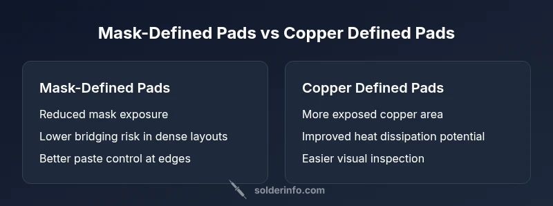
Solder mask defined pads are defined by a solder mask opening that sits slightly inside the copper pad edge. The exposed copper is smaller than the mask opening, leaving mask around the pad as a dam. This can reduce solder wicking and help control solder paste deposition on fine-pitch components. From a design perspective, SMD pads can improve predictability in mass production, reduce the risk of solder bridging, and facilitate stencil alignment because the mask dam provides a clear visual boundary for the paste deposition. For hobbyists, SMD can be easier to inspect under simple magnification since the mask provides a reference frame around the pad. The choice often hinges on pitch, paste stencil design, and the capabilities of the PCB fabricator.
What is copper defined (Cu-defined)?
Copper defined pads expose a defined area of copper that matches or slightly exceeds the mask opening. The copper geometry dictates the exposed area, not the mask dam alone. Copper defined pads typically yield larger exposed copper surfaces, which can improve heat dissipation for power components and can simplify certain inspection tasks where the pad edge is a focus. In addition, Cu-defined pads may allow more straightforward solder paste flow in some stencil designs, particularly when working with thicker pastes or larger pads. However, the broader exposed copper area can increase the risk of solder bridging in dense layouts if paste control isn’t precisely managed.
Design implications: Solder mask defined vs copper defined in practice
The choice between solder mask defined vs copper defined affects several design aspects: pad geometry, paste stencil interaction, and reflow behavior. SMD pads generally require tighter PCB fabrication tolerances and careful stencil alignment, especially for ultra-fine pitch packages. Cu-defined pads offer more copper surface for heat dissipation and can ease visual inspection but demand stricter control over stencil printing, paste volume, and reflow profile to prevent bridging. The decision should be guided by the component library and the assembly line’s capabilities. SolderInfo suggests that the interplay between paste type (no-clean vs halogen-free), stencil thickness, and mask dam dimensions plays a critical role in final solder fillet quality and reliability.
Manufacturing and quality considerations
Manufacturing tolerances, mask alignment accuracy, and paste deposition precision are central to a successful pad definition strategy. When using solder mask defined pads, ensure the mask alignment budget considers possible distortion during lamination and exposure; misalignment can reduce the intended dam effect and contaminate the pad. Copper defined pads require careful control of copper plating thickness and mask clearance to prevent excess exposure or inconsistent wetting. SolderInfo analysis shows that engaging with the fabrication house early, sharing fiducials, and validating with test coupons can reduce surprises during assembly. It is essential to review the PCB fab’s capabilities, including their mask expansion allowances and paste deposition tolerances, before finalizing a design.
Package and board-level decision criteria
The optimal pad definition often depends on the package and the board layout. Fine-pitch CSPs, QFNs, and µBGA devices commonly benefit from solder mask defined pads due to tighter bridging control, while larger QFP or power packages may perform better with copper defined pads for improved heat dissipation and easier inspection. Consider the alignment tolerance of your assembler and whether your stencil designer can reliably reproduce the intended pad geometry at the target pitch. In mixed-assembly boards, it may be advantageous to mix pad definitions, applying mask-defined pads for dense regions and Cu-defined pads where heat and accessibility are prioritized. SolderInfo emphasizes pre-production reviews with your assembler to validate the chosen strategy.
Practical guidelines for designers
To implement an effective pad-definition strategy, start with a baseline suited to your target package. For fine-pitch devices, prefer solder mask defined pads and align your stencil design to keep paste within the mask-defined boundaries. For larger pads or heat-intensive components, consider copper defined pads to maximize exposed copper for heat transfer and inspection. Always coordinate with your PCB fab to confirm mask clearance, copper thickness, and printed paste tolerances. Use test coupons to validate pad geometry and reflow behavior before committing to a full production run. In practice, maintain consistent design rules across the board and document any exceptions for the fabricator.
Troubleshooting and common pitfalls
Common issues include misalignment between mask openings and copper pads, inconsistent paste deposition at mask-defined boundaries, and unintended wetting on Cu-defined pads due to excessive exposed copper. Ensure your CAM tooling properly compensates for mask expansion and copper tolerances, and verify with optical inspection and X-ray checks when applicable. If a design exhibits unexpected bridging or tombstoning, re-evaluate the pad definition for those references and consult the fab for recommended mask dam sizes or copper pad dimensions. Regular design reviews and iterative prototyping can help catch issues early.
Validation and workflow integration
Integrate pad-definition decisions into the DFM (design for manufacturing) workflow. Include clear documentation in the bill of materials and assembly drawings about whether each pad is mask-defined or Cu-defined, their intended paste volumes, and any special stencil considerations. Run a circuit-board design rule check (DRC) focused on pad openings, mask clearance, and copper exposed areas. Engage in a pre-production run with a small batch to validate solderability, bridging risk, and heat dissipation performance. The end goal is a robust design that translates cleanly from the CAD model to the solder paste stencil to the reflow oven without surprises.
Comparison
| Feature | Solder mask defined pads | Copper defined pads |
|---|---|---|
| Pad exposure | Mask dam around pad reduces exposure | Exposed copper area larger |
| Solder paste control | Mask-defined edges guide paste and reduce wicking | Cu-defined exposure can complicate paste flow |
| Bridge risk (fine pitch) | Lower bridging risk with mask-defined pads | Higher bridging risk if paste control is weak |
| Heat dissipation | Less exposed copper, potentially lower heat dissipation | Better heat sinking with larger exposed copper area |
| Inspection ease | Mask boundary aids visual alignment | Exposed copper may improve visual heat/terminal inspection |
Advantages
- Reduces copper exposure and bridging risk in dense layouts
- Mask dam provides clear paste boundaries for repeatability
- Better control of solder fillets for fine-pitch parts
- Facilitates consistent assembly across high-volume runs
Cons
- Copper defined pads allow larger exposed copper for heat dissipation
- Cu-defined pads can complicate paste deposition control in tight spaces
- Mask-defined pads may require fab-specific mask clearances and checks
Neither pad definition universally outperforms the other; choose based on package, paste behavior, and fab capabilities.
Use solder mask defined pads for dense, fine-pitch regions to minimize bridging. Prefer copper defined pads where heat dissipation and inspection are priorities, but validate with your fabricator’s process.
Quick Answers
What is solder mask defined (SMD)?
Solder mask defined pads use mask openings that are smaller than or equal to the pad to constrain solder exposure. The mask dam around the pad helps control solder wicking and reduces bridging in dense layouts.
SMD pads use mask openings to limit solder exposure and reduce bridging in tight layouts.
What is copper defined (Cu-defined)?
Copper defined pads expose a defined portion of copper, with mask openings that can be larger than the copper pad. This increases exposed copper area and can aid heat transfer and inspection.
Cu-defined pads expose more copper for heat and inspection, but can affect paste behavior.
Which is better for fine-pitch components?
For ultra-fine pitch components, solder mask defined pads are often preferred to limit solder bridging. However, fab capabilities and stencil design are critical to success.
Mask-defined is usually better for very fine pitch, but check with your fab.
Can you convert from copper defined to mask defined?
Conversion involves adjusting both the copper pad geometry and mask opening. Work with the PCB fab to ensure mask clearance and tolerance are feasible for the target production run.
You can switch by updating copper and mask openings with your fab’s guidance.
How does pad definition affect rework and repair?
Mask-defined pads can make some rework techniques harder if the mask interferes with pad access, while Cu-defined pads generally provide easier access for certain repair procedures.
Mask definitions can impact access during rework; copper definitions may ease it.
Are there industry standards for pad definitions?
Standards vary by fab and application. Review IPC guidelines and consult your assembler for recommended practices on pad definitions, mask clearances, and paste deposition.
Standards are fab-specific; refer to IPC guidance and your fab’s practice.
Top Takeaways
- Prefer mask-defined pads for tight pitches and high-volume boards
- Cu-defined pads suit heat-sensitive or large-pad designs
- Coordinate with the fab to confirm mask clearance and copper thickness
- Validate with a pilot run and test coupons before full production
- Document pad-definition choices in the assembly drawings for clarity