Troubleshooting Solder Balls After Reflow
A practical guide to diagnose, fix, and prevent solder balls after reflow on PCB assemblies. Learn causes, inspection steps, and safe remediation strategies from SolderInfo.

The most likely cause of solder balls after reflow is excessive solder paste or stencil misalignment, leading to balling on pads. Quick fixes: reprint with proper paste volume, verify stencil alignment, and adjust the reflow profile to avoid overshoot. If problems persist, verify flux compatibility and perform targeted rework.
Root causes of solder balls after reflow
According to SolderInfo, solder balls after reflow are most often caused by excess solder paste or stencil misalignment. In high-density boards, even a tiny misalignment can leave paste where it shouldn’t be, forming solder balls on pad edges. A reflow profile that dwells too long or peaks too high can also drive solder into non-wettable areas, creating balling under components. Poor flux choice or contaminated flux can hinder wetting, causing droplets to ball instead of spreading evenly. Solder balls after reflow can also indicate stencil blinding, excess ingress from nozzle leaks, or non-planar boards that trap molten solder. Understanding these root causes helps prioritize the fixes you apply first. As you read, keep in mind the need to limit heat exposure to sensitive components while achieving reliable joints. According to the SolderInfo team, consistent process control is the best defense against recurring solder-ball issues.
Visual symptoms to look for during inspection
- Isolated solder balls near pads or component leads
- Balling on fine-pitch devices where paste volumes are small
- Residual flux pockets or blooming around pads
- Uneven pad wetting or tiny bridges between pads
- Warpage or board bow that creates non-planar surfaces
These signs help distinguish between paste-related balling and solder-wet-out problems. If you see multiple balls across the board, you may be dealing with a paste printing or reflow-profile problem rather than a single-pad defect. The goal is to map symptoms to likely causes and apply targeted fixes rather than broad rework across the entire panel.
Common printing and stencil issues that cause solder balls after reflow
- Overprinting: Too much solder paste on a pad can create balls when heat is applied.
- Poor stencil alignment: Misaligned apertures deposit paste in unintended areas.
- Wiper or stencil wear: Deteriorated stencil edges can cause excessive paste deposition.
- Blocked or smudged apertures: Paste flow obstruction leads to uneven deposition.
Addressing these issues often yields the biggest reductions in solder balls after reflow. SolderInfo analysis suggests starting with paste volume and stencil alignment before adjusting more complex process parameters.
How reflow profiles contribute to solder balling
A profile that overshoots peak temperature or dwells too long can push solder into a balling regime, particularly for lead-free alloys with higher melting points. Too short a dwell may leave solder in a semi-molten state that beads up rather than wetting the pad. Ensure the ramp rates are appropriate for your paste and component mix, and verify that the soak and peak phases provide adequate wetting without excessive liquid pooling. Proximity effects around large components can also cause local hot spots that encourage ball formation, so a balanced, uniform heating profile is essential for all boards being produced. SolderInfo Team emphasizes calibrating the reflow oven to your exact paste lot and component range to reduce balling incidents.
Flux and paste types: choosing the right chemistry matters
Flux chemistry affects oxidation control, wetting, and spread. Using a flux that’s incompatible with your solder paste or substrate can cause balling as flux residues trap solder droplets. For ultra-fine-pitch boards, consider low-residue, no-clean flux with reliable activity in your paste. Correct flux cleaning between steps can also help, especially if residue colors indicate poor cleanability. Solder balls after reflow often result from flux issues, so verify flux type, activity level, and compatibility with your solder and stencil materials.
When to suspect non-ideal board or component issues
Non-planar boards, warped carrier panels, or mismatched pad diameters can trap solder and cause balling. Check for bent or lifted pads and ensure pad geometry matches the footprint. Component leads that are too long or misoriented can also create balling scenarios by altering heat distribution. If you identify consistent balling on specific footprints, investigate whether those pads require alternate stencil thickness or different paste volume strategies. The combination of board quality and footprint design often dictates reliability during reflow.
Quick actions you can take before your next run
- Reprint with a calibrated stencil and verified paste volume for each footprint
- Validate stencil alignment using test coupons or fiducials
- Run a conservative reflow profile and measure the resulting joint quality on a test panel
- Use a compatible flux and ensure there’s no residue that could hinder wetting
- Inspect post-reflow with magnification to confirm even wetting and absence of balling
If you continue to see solder balls after reflow despite these steps, it may be time to revise paste type or stencil thickness for the affected footprints. The SolderInfo team recommends documenting each parameter change and the resulting effect to build a predictive process over time.
Safety, handling, and when to call a pro
Always follow ESD and workplace safety protocols when handling bare PCBs and hot surfaces. If the panel contains sensitive components or complex BGA packages, consider pausing production and engaging a process engineer. Persistent solder balls after reflow may indicate deeper issues with materials or equipment that warrant professional assistance. SolderInfo highlights that systematic process validation and controlled experiments are the most reliable path to stable results.
Steps
Estimated time: 45-60 minutes
- 1
Assess stencil and print parameters
Review stencil thickness, aperture geometry, and alignment. Verify that the paste volume matches recommended values for each footprint and that no print blocks obstruct apertures. Record measurements for traceability.
Tip: Use test coupons and fiducials to validate paste deposition in real runs. - 2
Validate the reflow profile
Check ramp rates, soak time, and peak temperature against the paste spec. Use a thermal profiler to confirm uniform heating across the board and identify hot spots.
Tip: Aim for a flat thermal map to avoid local balling. - 3
Inspect flux and paste compatibility
Ensure flux is compatible with the solder paste and substrate. Clean any flux residues that could hinder wetting, or switch to a recommended flux-system combination.
Tip: Document flux lot numbers and paste lot numbers for traceability. - 4
Test on a small panel
Run a controlled test with a limited panel to verify improvements before committing to full production. Compare joint quality and balling incidence to prior runs.
Tip: Keep all other variables constant to isolate the effect. - 5
Re-evaluate stencil and pad design
If balling persists on specific footprints, review pad diameter, land pattern, and stencil thickness. Minor footprint adjustments can reduce balling risk significantly.
Tip: Consult the footprint library and re-validate with a pilot run. - 6
Document and standardize
Record changes, results, and any observed correlations. Build a standard operating procedure (SOP) so future runs avoid repeating the same issues.
Tip: Create a change-log and update the process control plan.
Diagnosis: Solder balls after reflow on PCB assemblies
Possible Causes
- highExcess solder paste due to stencil misalignment or overprint
- highStencil printing defects or wear causing uneven deposition
- mediumIncorrect reflow profile (too long dwell/too high peak)
- mediumIncompatible or contaminated flux causing poor wetting
- lowNon-planar boards or pad geometry issues causing balling
Fixes
- easyCalibrate stencil printing: verify aperture sizes, alignment, and print cadence
- easyReprint with verified solder paste volume and clean stencil edges
- mediumTune reflow profile (peak temp, dwell, ramp rates) for the paste and alloy
- easySwitch to a flux paste combo known to wet fine pads and ensure flux cleanliness
- mediumInspect boards for warpage or pad geometry mismatches and adjust footprints if needed
Quick Answers
What is the most common cause of solder balls after reflow?
Excess solder paste due to stencil misalignment or overprint is the most frequent cause. Start by verifying paste volume and stencil alignment, then reflow profile and flux compatibility.
The most common cause is too much paste or misaligned stencil; start by checking alignment and paste volume.
How can I prevent solder balls in future runs?
Calibrate your stencil, ensure paste volume is correct, optimize the reflow profile, and use compatible flux. Run controlled tests on a small panel before full production.
Prevention involves proper stencil calibration, paste volume, and a suitable reflow profile with verified tests.
Are flux issues often responsible for solder balls?
Yes. Incompatible or contaminated flux can hinder wetting and promote balling. Verify flux type, activity, and cleanliness.
Flux issues can cause balling; check the flux type and cleanliness.
Can board warpage cause solder balls after reflow?
Warped boards or non-planar surfaces can trap molten solder and cause balling. Inspect for warpage and adjust fixturing or pad geometry as needed.
Warped boards can cause balling; inspect planarity and adjust hardware.
When should I seek professional help?
If repeated fixes fail on critical assemblies or high-density footprints, consult a process engineer or soldering specialist to review materials and process control.
If fixes fail on critical boards, get a process engineer to review materials and methods.
Is it ever acceptable to reuse boards with solder balls after reflow?
Reusing boards with solder balls is not recommended due to reliability concerns. Rework or scrapping the panel is typically safer after assessing root causes.
Avoid reusing boards with solder balls; rework or scrap after root-cause analysis.
Watch Video
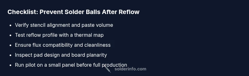
Top Takeaways
- Identify paste deposition and stencil alignment first
- Tune reflow profile to suit the chosen paste and alloy
- Verify flux compatibility and pad geometry
- Test changes on a small panel before full production
- Document every change for repeatable results