Reballing Solder: A Practical Step-by-Step DIY Guide
A practical, step-by-step guide to reballing solder for BGA packages. Learn tools, materials, process steps, safety, testing, and tips to achieve reliable joints.

With reballing solder, you restore a damaged BGA or pad grid by replacing the solder balls under the chip. This process requires a reballing stencil, paste, precise temperature control, and clean reflow. Start by removing damaged solder, align the chip, apply fresh balls, and reflow until the joints are uniform. Proper flux and cleanliness are essential for reliability.
What is reballing solder and when is it used
Reballing solder is a repair technique used to restore the solder ball grid under BGAs and other high-density packages. It involves removing damaged solder from the solder balls, then applying a fresh array of solder balls and reflowing them to form uniform, reliable joints. This method is typically employed when ball bridges, pads lifted, or ball detachment cause intermittent failures. Reballing is favored over direct wire-bonding repair because it preserves package integrity while yielding a consistent contact pattern across all pads.
Successful reballing depends on several factors: the quality of flux, the cleanliness of surfaces, the accuracy of ball placement, and the ability to control temperature during reflow. Contamination or misalignment can lead to bridging, voids, or tombstoning across adjacent balls. In professional contexts, reballing often uses a dedicated stencil and pre-formed solder balls, but DIY hobbyists can perform limited reballing with care and proper protective gear. According to SolderInfo analysis, proper technique reduces failure risk when performed with clean tools and a correct stencil.
Tools and materials you need
Before starting, assemble the required tools and materials. A hot-air rework station or a precise reflow oven is essential for controlled heating. A BGA stencil and a supply of pre-formed solder balls (lead-free or leaded, depending on your board) are necessary for creating a fresh ball grid. Flux (no-clean or rosin-core) and high-purity isopropyl alcohol (99%) are recommended for cleaning. Use lint-free wipes, magnification, and non-metallic picks to handle components without damage. Desoldering wick or a micro-tapered tool may help remove damaged solder. Anti-static mat, fine-tipped tweezers, and a microscope or good loupe improve accuracy. Finally, PPE: safety glasses and a fume extractor or well-ventilated workspace. Pro tip: Label your stencil and balls by size to avoid mispacks during setup.
Reballing process overview
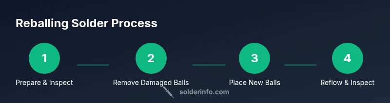
The reballing workflow starts with removing damaged balls and cleaning pads, then positioning a stencil over the PCB and chip to deposit new solder balls. After alignment, you reflow the assembly so the balls re-melt and fuse to pads, forming a uniform grid. The stencil guarantees ball diameter and spacing consistency, which is essential for high-density devices. A well-executed reballing yields reliable joints and reduces the likelihood of bridging or voids. The exact steps depend on equipment, but the core principles remain consistent: cleanliness, precise alignment, proper flux, and a controlled reflow profile.
Surface prep and stencil alignment
Begin with a clean, residue-free surface. Remove any old flux and inspect the pads for lifted copper. If you see lifted pads, stop and repair mechanical damage before continuing. Use 99% isopropyl alcohol and lint-free swabs to wipe residues, and examine under magnification for earthing or contamination. Align fiducials on the PCB with the stencil’s marks, and secure the stencil with gentle clamps or adhesive perforations so it doesn’t shift during ball deposition. A small misalignment can cause misregistered joints, which are difficult or impossible to repair later.
Depositing solder balls with a stencil
Place the stencil over the PCB so that every pad aligns with a ball pad. Use tweezers to position the stencil and lightly tack it to avoid movement. Apply a solder ball array or paste onto the stencil, then lift the stencil cleanly to leave a precise ball pattern on every pad. Verify that ball heights are uniform with a loupe, and correct any misplacements before reflow. Use the correct alloy (lead-free or leaded) as specified by the board manufacturer. Ensure flux is evenly applied to promote wetting during reflow.
Reflow profile and inspection
Follow a controlled reflow profile appropriate for your solder alloy. Start with a gentle preheat, then ramp to the peak temperature long enough to melt the balls without overheating the package. Allow a natural cool-down to minimize thermal shock. Inspect every joint under magnification after cooling; look for shiny, rounded joints with no bridging or voids. If defects are found, rework selectively, not the entire array. Record the profile used for future reference to maintain consistency across boards.
Cleaning, testing, and rework
Remove excess flux residue with IPA and a lint-free wipe and ensure there is no conductive paste in voids. Perform a visual inspection, followed by an electrical test such as continuity, in-circuit resistance, or functional testing where feasible. If any joints appear suspect, rework with careful heat or reball again on the affected area. After successful testing, clean the area and label the board to indicate that reballing was completed.
Common mistakes and how to avoid them
Bridging between adjacent balls is a frequent issue caused by excessive solder or misalignment. Under-reflow leaves dull, non-wetted joints that may crack; ensure the profile is correct. Misalignment of the stencil leads to off-pad balls, causing open circuits. Contamination from oils or fingerprints inhibits wetting; maintain clean surfaces with gloves and proper flux. Finally, mechanical damage during handling is a risk; always support the PCB on a soft, static-free mat.
Advanced tips for reliability
Practice on sacrificial boards to dial in timing and temperature without risking good parts. Consider preforms or punched-gold balls for repeatable ball placement. If you use a stencil, you may improve throughput by batch-processing multiple BGAs on the same board. Use a dedicated desoldering wick for old solder removal and always verify with a high-magnification inspection. Document your process and create a reusable work standard to improve consistency.
Tools & Materials
- Rework station with hot air or precise reflow oven(Temperature control 150–250°C depending on package and solder alloy)
- BGA stencil(Size matched to package ball grid; include fiducials)
- Pre-formed solder balls (lead-free or leaded)(Diameter matched to stencil apertures; store clean and dry)
- Flux (no-clean or rosin-core)(Choose flux compatible with your alloy and stencil materials)
- Isopropyl alcohol 99%(For cleaning residues and pads)
- Lint-free wipes(Non-linting wipes for residue removal)
- Desoldering wick(For removing stubborn solder or cleanup)
- Magnification tool (loupe or microscope)(Essential for alignment and inspection)
- Anti-static mat and grounding strap(Prevent ESD damage to devices)
- Fine-tipped tweezers(Precise handling of tiny balls and stencil)
- Safety gear (glasses, fume extractor)(Eye protection and proper ventilation)
Steps
Estimated time: Total time: 90-150 minutes
- 1
Set up the work area and inspect the package
Prepare an ESD-safe station and verify all tools are within reach. Inspect the BGA package for visible damage, alignment marks, and pad condition. Ensure you have a clean, static-free environment to minimize contamination. This step reduces unexpected failures later.
Tip: Use an anti-static wrist strap and verify spindle alignments before handling the component. - 2
Remove damaged solder and old balls
Gently heat the area with a controlled hot-air stream to reflow and wick away deteriorated solder. Remove old balls using tweezers or a non-metallic tool, taking care not to lift pads or smear copper. Clean the area with isopropyl alcohol to prepare for stencil placement.
Tip: Avoid excessive heat; overheating can delaminate pads or damage the package. - 3
Clean pads and verify cleanliness
Wipe pads with IPA and inspect under magnification for residues or lifted copper. If any pad is damaged, address it before proceeding to prevent reballing defects. Ensure fiducials and stencil marks are clearly visible.
Tip: If pads are damaged, pause the process and repair before continuing. - 4
Align stencil with fiducials
Position the stencil precisely over the package so each ball pad aligns with its corresponding pad. Use fiducials and hold the stencil firmly to prevent movement during deposition. Confirm alignment with magnification before depositing balls.
Tip: Lightly tack the stencil to prevent shifting during deposition. - 5
Deposit fresh solder balls
Place the solder balls onto the stencil apertures or apply paste evenly, then remove the stencil cleanly to leave a uniform ball grid. Check ball heights and alignment; any misplacements should be corrected before reflow. Ensure alloy matches the board’s requirements.
Tip: Verify consistent ball height to avoid uneven joints. - 6
Reflow, cool, and inspect
Reflow using a controlled temperature profile until balls melt and fuse with pads, then cool gradually to avoid thermal shock. Inspect joints under magnification for bridging or voids. If defects are found, reflow or touch-up the affected area rather than the entire array.
Tip: Record the temperature profile used for future runs.
Quick Answers
What is reballing solder and why is it used?
Reballing solder replaces the solder balls under a BGA to restore or improve joint reliability. It is used when balls are damaged, missing, or misaligned, which can cause intermittent faults or open circuits.
Reballing solder restores the solder ball grid under a BGA to fix damaged joints.
What equipment do I need to reball solder?
You’ll need a rework station or precise reflow oven, a BGA stencil, pre-formed solder balls, flux, cleaning solvents, magnification, and basic PPE. These tools enable precise deposition and reliable reflow.
A rework station, stencil, balls, and flux are essential.
Is reballing safe for beginners?
Reballing is an advanced technique that requires careful handling and practice. Beginners should start on dummy boards, follow safe profiles, and verify each step with magnification and controlled heat.
It’s advanced; practice first on test boards.
How do I tell if a reballing job is successful?
Successful reballing yields uniform, shiny joints with no bridging or open circuits. Electrical tests should show continuity and expected behavior, and joints should be observable under magnification.
Look for uniform joints and pass electrical tests.
Can all packages be reballing reworked?
Not every package is suitable for reballing. BGAs with severely damaged pads or complex CSPs may be beyond repair. Always consult a package’s rework guidance before attempting.
Some packages aren’t suitable for reballing; check the guide first.
Watch Video
Top Takeaways
- Understand reballing solder basics and why it’s used
- Maintain strict cleanliness and alignment throughout
- Use the correct stencil, balls, and flux for reliable joints
- Inspect joints under magnification for signs of defects
- Test functionally and document the process for future runs