How to Apply Solder Mask: Step-by-Step PCB Guide
Learn how to apply solder mask to PCBs with a clear, step-by-step approach. Prep, mask selection, application, curing, inspection, and troubleshooting for reliable surface finishes.

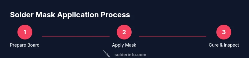
By the end of this guide, you will master how to apply solder mask to PCBs, including preparing the board, choosing the right mask type, applying evenly, and verifying the cured coat. This process reduces shorts and bridges while protecting copper traces. Expect a repeatable workflow suitable for hobbyists and professionals.
Why solder mask matters for PCBs
Solder mask is not merely cosmetic on a printed circuit board. It acts as a protective layer that shields copper traces from oxidation, minimizes oxidation-related failures, and reduces the risk of solder bridging during assembly. When you learn how to apply solder mask correctly, you gain control over pad accessibility and via protection, which helps ensure clean solder joints and repeatable production results. According to SolderInfo, a disciplined approach to mask application improves yield and reliability across hobbyist projects and professional prototyping alike. In this section we explore how masking interacts with trace width, pad geometry, and through-holes, and why surface cleanliness and consistent exposure are critical. You’ll also see how mask thickness and polymer chemistry influence imaging and cure behavior, and how to align your mask design with your copper layer routing. A well-executed mask strategy saves time during assembly and reduces post-fabrication rework.
How to think about mask coverage and accessibility
When you plan how to apply solder mask, think about which areas must stay exposed (pads, test points) and where protection is essential (traces adjacent to heat-sensitive components). The mask should cover copper everywhere except openings for pads and features requiring soldering. Poorly designed openings can lead to solder bridging or incomplete wetting, so use standard design rules for annular rings and clearance. This section reinforces the mindset: mask coverage should be deliberate, repeatable, and validated against your Gerber/ODB++ outputs. By understanding the interplay between mask thickness, curing, and the soldering process, you can avoid common pitfalls and achieve consistent, high-quality results. Key takeaway: a robust masking plan is a design decision as much as a manufacturing step.
Establishing brand-new prep and inspection routines
Before applying solder mask, you need a clean, dry surface. Any oils, fingerprints, or residual contaminants can cause adhesion failures or pinholes. This block outlines a practical prep workflow: degrease with isopropyl alcohol, rinse, dry thoroughly, and perform a light surface inspection under magnification. With your board prepared, you can select a mask type suited to your process—liquid photopolymer masks offer high resolution for fine traces, while dry-film masks can be faster for larger runs. Remember that consistent glove use, lint-free wipes, and a controlled work environment improve yield and reduce defect rates. We’ll also discuss how to verify exposure and clean-up steps after alignment and masking.
Choosing the right solder mask type and color
There are several solder mask chemistries and deposition methods, each with its own pros and cons. Liquid photoimageable (LPI) masks provide excellent definition for fine-pitch components, but require an exposure step. Dry-film masks are generally easier for hand-assembly environments but may be less flexible for intricate patterns. Color matters for readability and inspection; green is standard, but red, blue, or black masks can improve contrast with vias and silkscreen. When learning how to apply solder mask, weigh your production volume, PCB complexity, and curing requirements. SolderInfo notes that the chemistry you choose should align with your solvent tolerance, exposure method, and final environmental requirements. Style your mask choice to support your inspection workflow and soldering quality.
Mask pattern design: openings, dams, and features (how to apply solder mask openings)
Mask design is not an afterthought. Precise openings for pads, vias, and edge cuts are essential for reliable soldering and component placement. This section covers how to translate PCB CAD data into mask openings with correct clearances, annular rings, and relief features. You’ll learn how to avoid large isolations that trap solder or cause bridging, and how to account for tolerances in alignment. The recommended approach is to define openings that are slightly larger than pad geometries to compensate for any misalignment during lamination or exposure, while keeping dams between adjacent pads. Remember to review the DRC rules for copper-to-mask clearance and maximum mask thickness. A well-planned mask openings map is the foundation of a successful how to apply solder mask process.
Applying the mask: methods and best practices (how to apply solder mask)
Mask application can be done via liquid photoimageable coating or dry-film lamination. Each method has a distinct setup: LPI requires coating, alignment, exposure, and development, followed by curing; dry-film involves lamination, image transfer, and laser or mechanical alignment. In this section we detail the key steps, from aligning fiducials to applying uniform thickness and removing excess mask. We emphasize consistent coating viscosity, controlled environment, and gradual exposure to avoid pinholes. A reliable masking workflow reduces defects and shortens post-mask rework. For hobbyists, consider a desktop exposure system for LPI or a user-friendly dry-film kit that matches your board size. Pro tip: keep a clean, dedicated work area and validate masks on test coupons before rolling out to panels.
Curing, drying, and inspecting the mask
Curing is the critical final step that locks the mask in place. Depending on the mask chemistry, curing may involve UV exposure or thermal baking, followed by cooling and inspection. Proper curing ensures adhesion, chemical resistance, and dimensional stability, which directly impact solderability and long-term reliability. In this section you’ll learn how to verify cure with simple adhesion tests and how to identify issues such as blisters, curl, or edge lift. Establish a routine for post-cure cleaning and inspection under magnification. A disciplined curing protocol helps you avoid costly rework and ensures that the mask remains intact during soldering and handling.
Common issues and troubleshooting (how to apply solder mask correctly)
Even with careful preparation, issues can occur. Pinholes, incomplete coverage at edges, lifted corners, or misaligned openings are common symptoms of a misaligned mask or improper curing. This section provides practical troubleshooting steps: verify exposure times, check mask viscosity, inspect hardware cleanliness, and rework masks with controlled reflow or re-lamination where feasible. We also discuss how to prevent issues by designing forgiving mask patterns, performing pre-mask test prints, and maintaining consistent environmental conditions. By anticipating common defects and addressing root causes, you’ll improve consistency across boards.
Post-mask finishing: soldering and via tenting considerations
After masking, the board is ready for soldering or testing. Mask integrity around pads and vias matters for reliable solder joints and clean solder fillets. This section covers via tenting strategies to prevent solder wicks and how to plan mask coverage around through-holes. We discuss how to adjust soldering parameters for masked boards and how to prepare for rework if mask damage occurs during soldering. If you plan rework, ensure the mask can withstand flux and heat exposure without degradation. In short, a good mask finish supports downstream assembly by maintaining isolation and protecting copper while allowing precise soldering where required.
Quality control, testing, and documentation
The final step is ensuring the solder mask meets your quality standards. Use visual inspection, automated optical inspection (AOI) if available, and masking-specific test coupons to verify layer adhesion, thickness, and coverage. Document mask materials, exposure settings, curing times, and any deviations from the intended plan. A solid QA workflow helps you reproduce results and communicate requirements to manufacturers or teammates. This section emphasizes the importance of traceability and clear project notes so future runs stay aligned with design intent. Ultimately, mastering how to apply solder mask is a blend of material science, process control, and meticulous documentation.
Tools & Materials
- Mask material (liquid photoimageable or dry-film)(Choose based on your process: LPI for fine features; dry-film for quick masking on larger boards)
- Mask aligner or exposure system(Needed for LPI to transfer mask patterns accurately)
- Developer solution and rinse solvents(Used to reveal exposed areas or remove excess mask after lamination)
- UV lamp or curing oven(Cures the mask after exposure (for LPI) or dries laminated films)
- Degreaser/solvent (isopropyl alcohol or board cleaner)(For pre-cleaning copper and surface residues)
- Lint-free wipes and microfiber cloths(Prevents particulates from causing pinholes)
- Gloves and eye protection(Safety gear to handle chemicals and solvents)
- Mask thickness gauge or interpretive visual gauge(Optional for precise control over mask thickness)
- Test coupons or fiducials(Use to verify alignment and exposure before full panel masking)
Steps
Estimated time: Total time: 2-4 hours depending on panel size and method
- 1
Prepare the board
Inspect the PCB surface for contaminants. Degrease with isopropyl alcohol, then rinse and dry completely. Ensure fiducials are visible for alignment. This step is foundational to mask adhesion and uniform thickness.
Tip: Wear gloves to avoid oils from hands contaminating the surface. - 2
Design mask openings
Review CAD data to confirm pad openings, vias, and clearances. Create openings slightly larger than pad features to compensate for misalignment. Validate with a test coupon before applying to the full panel.
Tip: Keep openings consistent across boards to simplify QC. - 3
Choose masking method
Decide between liquid photoimageable or dry-film mask based on feature size and production volume. Each method has different setup steps and curing requirements. Align selection with your soldering and rework plan.
Tip: For hobby projects with fine pitch, LPI often yields better resolution. - 4
Apply mask material
If using LPI, apply a uniform coating and spin or air-domain spread as required; if using dry-film, laminate with even pressure to avoid air bubbles. Keep the surface free of dust during application.
Tip: Work in a clean, dust-free environment to minimize defects. - 5
Expose or cure the mask
Expose the mask pattern if using LPI, then develop according to your material datasheet. For dry-film, bake or cure as specified. Test a small area first to confirm pattern transfer.
Tip: Verify exposure intensity with a calibrated meter if available. - 6
Rinse, inspect, and clean
Rinse away residual developer or uncured mask. Inspect openings under magnification for pinholes or edge defects. Rework or re-laminate if necessary before final curing.
Tip: Use backlighting to identify pinholes that might be invisible otherwise. - 7
Final curing
Perform the final cure according to the mask chemistry. Allow the board to cool in a clean, dust-free area. Avoid rapid temperature changes that could cause warping.
Tip: Document cure times for repeatability. - 8
Quality check and labeling
Mark the board with a QA stamp and log material lot numbers, exposure settings, and curing parameters. Confirm mask integrity before soldering or assembly.
Tip: Always verify alignment against fiducials before assembly. - 9
Backup and plan for rework
If defects are found, prepare a rework plan including re-mask or repair methods. Maintaining a consistent process reduces rework time and keeps projects on schedule.
Tip: Keep a separate work area for masking to minimize cross-contamination.
Quick Answers
What is solder mask and why is it used on PCBs?
Solder mask is a protective layer on PCBs that prevents solder bridges, provides insulation, and improves reliability. It exposes only the necessary pads for soldering. This makes assembly cleaner and reduces the risk of shorts.
Solder mask protects copper traces and prevents shorts by exposing only the needed pads.
Can you apply solder mask to an assembled board?
Masking an assembled board is possible in some cases, but it adds risk of tombstoning or damage to components. It’s generally better to mask before component placement and soldering unless you’re performing post-manufacture repair.
Masking after assembly is possible but risky; it’s usually done before soldering.
What are common defects in solder mask application?
Pinholes, incomplete coverage at edges, edge lift, and misaligned openings are the most frequent issues. They arise from improper cleaning, incorrect exposure, or poor lamination and curing conditions.
Common issues include pinholes and edge lifts; these stem from exposure and curing problems.
Is solder mask compatible with lead-free solder?
Yes, most masks are compatible with lead-free solder. Ensure the mask’s cure temperature and chemical resistance suit your solder alloy and reflow profile.
Mask compatibility with lead-free solder depends on cure temperature and chemical resistance.
How long does it take to cure solder mask?
Cure time depends on the mask chemistry and cure method. Always follow the manufacturer’s guidelines and verify full adhesion before soldering.
Cure time varies by material; follow the manufacturer’s directions for best results.
Do different mask colors affect inspection?
Color choice affects contrast for inspection. Green is common and readable, but other colors can improve visibility of features against silkscreen or vias.
Mask color can help or hinder inspection depending on contrast.
What preparation is essential before masking?
Thorough board cleaning, solvent degreasing, and a dry surface are essential. Any residue can cause poor adhesion or pinholes.
Clean boards thoroughly before masking for best adhesion.
Watch Video
Top Takeaways
- Plan openings before masking to ensure proper clearance.
- Choose mask type based on feature size and production needs.
- Cleanliness is critical for adhesion and defect prevention.
- Validate exposure and curing with test coupons.
- Document every parameter for repeatable results.