DIY Solder Mask: A Practical Guide for Hobbyists
Learn to apply a reliable DIY solder mask on PCBs. This step-by-step guide covers surface prep, masking options, curing, and troubleshooting for reliable, solder-safe results.

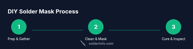
By following these steps you’ll learn to apply a DIY solder mask to PCBs using common materials. You’ll prep the board, create a stencil, apply masking liquid or tape, and cure it for a reliable solder mask. This guide covers safety, surface prep, mask options, curing, and troubleshooting for hobbyists and professionals alike.
What is solder mask and why DIY?
A solder mask is a protective, often colored, layer applied over copper traces on a printed circuit board (PCB) to prevent solder bridges, oxidation, and accidental shorts. For hobbyists, a DIY solder mask can be a cost-effective way to prototype boards or protect small runs without ordering pre-coated boards. DIY options include liquid solder mask formulations that cure with air or UV light, and dry-film or Kapton-tape approaches for edge-defined openings. When used correctly, a DIY solder mask provides similar electrical insulation and solder-pinning benefits as commercial masks, while offering flexibility for small projects. The SolderInfo team notes that choosing the right mask type for your board’s material and environmental exposure is crucial for long-term reliability.
Safety and environmental considerations
Working with masking liquids and solvents requires attention to ventilation, PPE, and handling. Always work in a well-ventilated area or under a fume hood. Wear gloves resistant to adhesives and solvents, and eye protection when dispensing liquids. Some epoxy or UV-curable masks can irritate skin or emit fumes during curing; read the product data sheet and follow manufacturer guidance. Keep solvents away from heat sources and open flames, and dispose of rags and waste according to local regulations. If you’re unsure about the chemical compatibility with your PCB substrate, opt for a low-odor, low-toxicity option and test on a sacrificial board first.
Materials and tools you’ll need (at-a-glance)
- Solder mask liquid or dry-film mask (choose UV-curable if you have a curing lamp)
- Kapton/Polyimide tape or a precision stencil
- Fine brush, squeegee, or applicator tool
- Isopropyl alcohol (IPA) and lint-free wipes
- PPE: gloves, safety glasses
- Optional: UV curing lamp, magnification tool
- Clean work surface and good lighting
Choosing between liquid masks and tape depends on board complexity and required edge precision. Liquid masks are great for uniform coats, while tape or stencil methods excel with intricate pad openings. The goal is a consistent coat thickness with crisp boundaries.
Preparing the PCB surface for masking
Begin with a clean, dry PCB. Remove grease, fingerprints, and oxidation using IPA or a dedicated PCB cleaner. If the copper fins show oxidation, lightly abrade with a non-metallic pad and re-clean. Ensure the board is completely dry before applying any mask. Any residue or moisture can cause poor adhesion or pinholes. For best results, test your masking method on a spare board to dial in coat thickness and cure time.
Creating a stencil or edge definition for openings
For clean pad and via openings, you’ll need a precise stencil or edge-defined masking approach. Kapton tape can be cut to expose only the solderable copper, while a laser-cut or printed stencil can guide mask application. Align the stencil to fiducials and confirm board orientation before applying the mask. If edges bleed under, rework the boundary by adding a narrow mask border and resealing with the mask layer.
Applying the mask: liquid mask application technique
Apply the masking liquid in thin, even passes to avoid runs and sags. Use a small brush for edges and a squeegee for larger areas if using screenable liquid. Allow the first coat to set briefly before adding a second lighter coat for uniform coverage. Thicker coats can trap solvents and cause adhesion failure. Maintain a clean edge to prevent masking material from creeping onto the pads.
Curing, drying, and initial inspection
Curing methods vary by product: some masks cure with ambient air, others require UV exposure. Follow the data sheet for cure times and temperatures. After curing, inspect under magnification for pinholes, edge bleeding, or bare copper. If you find defects, lightly abrade the surface, re-clean, and apply a second mask layer following the same steps. A well-cured mask should feel firm to the touch and resist mild solvent exposure.
Troubleshooting common DIY solder mask issues
Pinholes, pin bleed, or uneven edges usually stem from improper surface prep, thick coats, or uneven cure. To fix pinholes, apply a thinner second coat, ensuring complete drying. If edges are not sharp, adjust stencil alignment and consider a tape mask with tighter boundary control. For masking liquids, ensure compatibility with your substrate and avoid over-diluting adhesives. For a robust result, practice on scrap boards and gradually increase complexity.
Best practices for different board types and scale
Small prototype boards benefit from tape-based masking for precise edges, while larger boards can benefit from liquid masks for uniform coverage. For boards with dense pad patterns, plan openings ahead of time and use a stencil to maintain consistent margins. Always test cure times on a sacrificial board to avoid under- or over-curing, which can compromise adhesion and solderability.
Tools & Materials
- Solder mask liquid or UV-curable mask(Choose UV-curable for quicker curing and consistent results)
- Kapton/polyimide tape or precision stencil(For edge definition and openings)
- Fine brush or squeegee(For even application of liquid mask)
- Isopropyl alcohol (IPA) and lint-free wipes(Surface cleaning and degreasing)
- Acetone or PCB cleaner (if needed)(For stubborn residues)
- Gloves and safety glasses(Protect skin and eyes from solvents)
- UV curing lamp or strong confines for air-dry mask(Depends on mask type)
- Magnification tool (optional)(Helpful for fine features)
- Clean work surface and good lighting(Essential base condition)
Steps
Estimated time: Estimated total time: 90-150 minutes
- 1
Prepare workspace and gather supplies
Set up a well-ventilated area with good lighting. Gather all materials so you don’t interrupt the workflow. Wipe the work surface and tools with IPA before starting.
Tip: Double-check that your mask type is compatible with your PCB substrate to avoid adhesion issues. - 2
Clean and degrease the PCB
Wipe the PCB with IPA to remove oils and fingerprints. Use a clean brush to reach tight areas around pads. Let the board dry completely before applying mask.
Tip: For stubborn residues, a quick light scrub with a non-metallic pad helps improve adhesion. - 3
Mask the non-solder areas
Apply Kapton tape or lay down a stencil to protect areas that must remain unmasked. Verify alignment with fiducials and trim edges for a clean boundary.
Tip: Mask edges should be tight but not overlapping pad openings to prevent bleed. - 4
Apply the solder mask liquid evenly
Dip or brush mask across the masked areas in thin passes. Allow each layer to set briefly before applying the next for uniform coverage.
Tip: Keep coats thin to minimize pooling and reduce cure time. - 5
Define openings for pads and vias
Use a stencil or precise cutting method to expose copper pads and vias. Ensure openings are crisp and edges are well-defined.
Tip: Test fit a sacrificial board to validate boundary accuracy before finalizing. - 6
Cure the mask
Cure according to the product instructions—UV light for UV-curable masks or air-dry for solvent-based masks. Avoid handling until fully cured.
Tip: Rotate the board during UV exposure to ensure uniform curing. - 7
Inspect the coating
Check for pinholes, blisters, or uneven thickness under magnification. Handle the board gently to avoid disturbing the mask.
Tip: If defects are found, rework on a sacrificial board before applying to the final PCB. - 8
Remove masking materials and final checks
Carefully remove tape or stencil. Wipe edges with IPA and re-check pad visibility. Confirm mask integrity before soldering tests.
Tip: Keep a spare mask layer handy for quick touch-ups during prototyping.
Quick Answers
What is a solder mask and why would I DIY it?
A solder mask is a protective layer over copper traces that prevents solder bridges and oxidation. DIY solder mask can be a practical option for prototypes or small runs when commercial masks aren’t necessary or affordable.
A solder mask protects traces and helps prevent shorts. For DIY boards, masking is a practical, budget-friendly option for quick prototyping.
Can I use household materials to create a mask?
Household materials are generally not recommended for reliable solder masking. Use purpose-made solder mask liquids or dry-film tapes designed for electronics to ensure proper adhesion and solderability.
Household materials aren’t reliable for solder masks. Use proper electronics-grade masking products for best results.
Will a DIY mask affect PCB solderability?
If applied correctly and cured fully, a DIY mask should not hinder soldering on exposed pads. Ensure openings are clean and masks do not cover pad areas.
If you follow the steps and cure properly, soldering should work as normal on exposed pads.
How long does curing take?
Cure times depend on the mask type and environmental conditions. UV-curable masks cure quickly under proper exposure; solvent-based masks may air-dry over several minutes to hours.
Cure time varies by product; UV masks cure fast under light, others take longer to dry.
What are common DIY mask pitfalls?
Common issues include pinholes, edge bleed, and incomplete curing. These are usually due to surface prep gaps, too thick coats, or insufficient curing.
Watch for pinholes and edge bleed, and ensure complete curing for best results.
Watch Video
Top Takeaways
- Plan openings before masking to ensure clean pads.
- Apply thin, even coats for uniform adhesion.
- Cure thoroughly before handling the board.
- Test and practice on sacrificial boards first.
- Choose masking method that suits board complexity.