Mask UV Solder PCB BGA Guide: From Prep to Finish
Learn how to apply UV-curable solder mask on PCBs with BGA components. A step-by-step, safety-conscious guide covering materials, alignment, curing, and inspection from SolderInfo.

Applying a UV-curable solder mask to a PCB with BGA footprints protects copper traces during reflow and makes rework safer. According to SolderInfo, selecting a mask with strong adhesion, chemical resistance, and precise aperture control is essential for high-density BGA patterns. The SolderInfo team emphasizes that alignment accuracy, surface prep, and cleanup set the foundation for a reliable mask. When done well, the UV mask helps prevent solder bridges, avoids shorts, and preserves pad integrity during final assembly. This approach also reduces post-reflow touch-ups and simplifies quality inspection, especially on lead-free boards. By planning apertures carefully and validating material behavior, you improve yield and reduce rework risk across multiple boards.
Why mask uv solder pcb bga
Masking a PCB with BGA footprints using a UV-curable solder mask protects copper traces during reflow and makes rework safer. According to SolderInfo, selecting a mask with strong adhesion, chemical resistance, and precise aperture control is essential for high-density BGA patterns. The SolderInfo team emphasizes that alignment accuracy, surface prep, and cleanup set the foundation for a reliable mask. When done well, the UV mask helps prevent solder bridges, avoids shorts, and preserves pad integrity during final assembly. This masking strategy also reduces post-reflow touch-ups and makes quality inspection more straightforward. Consider how environment, storage, and mask handling influence consistency across production boards, especially in lead-free soldering contexts.
Material choices: UV-curable solder mask formulations and compatibility with BGA
Choosing a UV-curable solder mask requires balancing wettability, adhesion, chemical resistance, and line/space definition to fit fine-pitch BGA pads. Look for masks labeled for electronics use with good solvent resistance and stable exposure after curing. SolderInfo analysis shows that some masks shrink slightly during cure, which can alter aperture sizes on dense BGA footprints. Always verify manufacturer data on dielectric constant, glass transition temperature, and compatibility with your solder alloy (lead-free or otherwise). For multi-layer boards, ensure the mask layer maintains adhesion through temperature cycles and cleaning processes. End-use environment, storage conditions, and work-in-progress handling should guide material selection.
Design considerations: mask openings, pad clearance, and via tenting for BGA
Define apertures for each BGA pad precisely, leaving enough clearance to prevent shorts while ensuring reliable solder deposits. Consider tenting vias that lie under the BGA area to reduce solder wick and contamination risk. Maintain consistent layer-to-layer alignment by using fiducials and a calibrated exposure stop. The mask edge around pads should be smooth, with minimal edge serration that can trap flux or solvents. For lead-free processes, verify that mask thickness and opening size do not impede solder flow or echo flux management. Good design thinking reduces post-reflow defects and simplifies inspection.
Preparation steps: cleaning, stencil alignment, and surface prep
Start with a clean, residue-free PCB surface. Use lint-free wipes, isopropyl alcohol, and a static-safe tray to prevent particles from landing on pads. Align any stencil or mask film using verified fiducials; misalignment here is a common cause of open/short defects after curing. Ensure the board is dry before application and avoid touching pad surfaces with bare hands. If you are reworking a board, verify pad integrity and any rework debris before masking. The goal is a uniform base layer that adheres strongly to copper and solder mask materials.
Application methods: spin-coating, screen-printing, and UV-curable films
There are several ways to apply UV-curable solder masks depending on equipment and board geometry. Spin-coating offers uniform coverage for flat boards but can be less controllable around BGA lands. Screen-printing with a dedicated stencil gives precise apertures for high-density patterns but requires careful stencil alignment. UV-curable films provide added control for double-sided boards and complex rework. Regardless of method, ensure consistent film thickness, minimize air bubbles, and keep the mask cure path free from dust. If you use a film, align carefully to the fiducials and press evenly to secure. For BGA, plan for adequate mask removal around pads while preserving the mask’s protective function.
Curing and post-cure inspection: UV exposure, post-bake, rework-friendly inspection
Cure the mask using the recommended UV wavelength and exposure energy for your material. After curing, inspect apertures for uniformity and any shrinkage that could affect pad exposure. Post-bake methods may be required to achieve final mask hardness; follow the mask supplier’s guidance. Inspect under magnification for pinholes, edge irregularities, or trapped air. Verify that via tenting is consistent and that BGA pads remain clearly exposed where needed. Document any deviations for future process improvements.
Masking challenges with BGA rework and reflow
BGA work introduces unique masking challenges: tight pad pitch, thermal cycling, and potential flux intrusion. Ensure mask thickness does not impede heat transfer or cause poor wetting at the pads. For rework scenarios, consider temporary mask removal only where necessary, and plan for reapplication after component replacement. Always keep a clean, dry rework area and use static control measures to avoid data loss on fine-pitch components. The mask should endure multiple reflows without cracking or delaminating.
Testing and quality checks
Perform a simple functional check by inspecting with a loupe or microscope to ensure mask openings align with BGA pads and traces. Confirm there are no shorts or excessive mask bleed near pad edges. A test coupon with a BGA footprint can be helpful to verify adhesion and exposure in a controlled sample before applying to a full board. Maintain traceable records of material lot numbers and exposure times for quality control.
Safety, handling, and disposal of UV mask materials
UV-curable solder mask materials contain solvents and photoinitiators that require proper ventilation and PPE. Work in a well-ventilated space and use gloves when handling uncured masks. Follow local regulations for disposal of chemical waste and cured mask scraps. Store materials away from heat sources and direct sunlight to preserve shelf life. Always check the material safety data sheet (MSDS) for hazards and first-aid measures. SolderInfo emphasizes safe handling as a core part of the process.
Tools & Materials
- UV-curable solder mask (LPI) material(Choose a material compatible with BGA pad openings and lead-free solder processes)
- UV exposure lamp or lamp array(Ensure intensity matches mask specification)
- Fiducials and alignment marks(Used for precise alignment of mask openings)
- Lint-free wipes and isopropyl alcohol(For cleaning copper surfaces before masking)
- Anti-static mat and wrist strap(Reduce particle contamination and ESD risk)
- Mask alignment tool or jig(Optional but helpful for tight BGA patterns)
- Gloves, safety glasses, and ventilation(Personal protective equipment)
- Magnification aid (10x-60x)(Inspect mask openings around pads)
- Solder flux compatible with mask(Use flux that works well with masked surfaces)
- Mask film (if using film approach)(Provide controlled masks for complex boards)
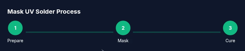
Steps
Estimated time: 3-5 hours
- 1
Set up workspace
Prepare a clean, static-free area with proper ventilation. Gather all required tools and materials. Verify fiducials and mask sheets are ready before starting.
Tip: Use an anti-static mat and keep the area dust-free. - 2
Clean board surfaces
Wipe copper areas with lint-free cloths and isopropyl alcohol to remove oils and oxides. Ensure pads remain dry before masking.
Tip: Avoid touching pads with bare hands to prevent contamination. - 3
Align mask openings
Place the mask or stencil on the board using fiducials. Verify alignment edges with magnification. Lock the mask in place if using a jig.
Tip: Double-check alignment marks before exposure. - 4
Apply mask material
For liquid mask, deposit evenly and in small amounts to control thickness. For film, align and press gently to remove air bubbles.
Tip: Aim for uniform thickness around pad edges. - 5
Cure the mask
Expose under UV light for the recommended duration. Avoid overheating the board during cure.
Tip: Monitor exposure time carefully to prevent over-curing. - 6
Inspect and verify
Inspect apertures with a loupe to ensure proper exposure. Check for pinholes, bridging, or edge irregularities near pads.
Tip: Record any deviations and retest on a coupon board.
Quick Answers
What is UV solder mask and why is it used on BGA PCBs?
A UV-curable solder mask provides insulation and protection for copper features while exposing pads for soldering. It helps prevent shorts and bridges around dense BGA patterns.
A UV-curable solder mask insulates copper and exposes pads for BGA soldering, helping prevent shorts and bridges.
Can I reuse standard solder mask for BGA, or must I use a UV-curable type?
For high-density BGA work, UV-curable masks offer better precision, adhesion, and process control. Standard masks may lack the necessary aperture repeatability and cure stability.
UV-curable masks give you better precision and stability for dense BGA patterns.
How do I ensure mask alignment with BGA pads?
Use fiducials, a calibrated exposure stop, and magnification to verify alignment before exposure. Lock the mask to prevent movement during curing.
Use fiducials and alignment marks to confirm mask placement before curing.
What safety precautions are essential when working with UV mask materials?
Work in a ventilated area and wear PPE. Follow MSDS guidance for photoinitiators and solvents, and dispose of waste according to regulations.
Ventilate the area and wear PPE; follow the material safety data sheet for photoinitiators and solvents.
How can I test a mask process before applying it to production boards?
Create a test coupon with BGA footprints to validate adhesion, opening accuracy, and cure behavior before committing to full boards.
Use a test coupon to validate adhesion and aperture accuracy before full boards.
Watch Video
Top Takeaways
- Plan mask coverage carefully to protect critical pads
- Use proper alignment and cleaning to avoid defects
- Cure under correct UV exposure to ensure durability
- Verify mask openings and tented vias before reflow