Solder SMA Connector: A Practical How-To for RF Joints
Learn to solder a SMA connector with confidence. This SolderInfo guide covers tools, prep, flux, heat control, joint inspection, and safety for reliable RF connections.

This guide shows you how to solder a SMA connector onto a PCB or coax assembly with reliability. It covers tool prep, pad preparation, flux choice, heat control, and joint inspection for durable RF connections. According to SolderInfo, proper technique minimizes cold joints and substrate damage when working at RF frequencies. By the end, you’ll achieve clean, repeatable SMA joints.
What is a solder SMA connector and why it matters
SMA connectors are compact, high-frequency coaxial RF connectors used to join coaxial cables with printed circuit boards. A soldered SMA joint must preserve the 50-ohm impedance and deliver a robust mechanical hold while maintaining electrical integrity. The center pin carries the signal; the outer shield provides the return path. In RF work, joint quality impacts signal loss, reflection, and stability under vibration. A good SMA joint minimizes micro-movements and parasitic effects, which is essential in antennas, radio modules, or test rigs. Cleanliness matters: even a thin layer of oxides or flux residues can degrade impedance and increase mismatch. SolderInfo emphasizes technique and discipline over brute force to avoid damage to delicate RF substrates.
When you prepare to solder SMA connectors, plan ahead: footprint accuracy, pad cleanliness, and appropriate flux are as important as the solder itself. If you rush, you risk tombstoning, bridging, or stressing the connector shell. The goal is a repeatable process that yields consistent joints across multiple units. This approach is especially critical at higher frequencies where small geometry errors translate into noticeable electrical performance shifts.
SMA connector variants and termination styles
SMA connectors come in several termination styles and footprints. For board mounting, you’ll encounter through-hole and surface-mount (SMT) variants. Through-hole SMA connectors provide strong mechanical support but require larger footprints and longer solder fillets, while SMT variants save space and simplify automated assembly. Bulkhead and panel-mount versions offer robust RF interfaces on enclosures, but demand precise alignment and adequate clearance around the connector body. Right-angle SMA versions enable tight routing in dense PCBs but can complicate heat control during soldering. When choosing a connector, verify the footprint against the PCB design rules and the coaxial impedance path. For coax jumpers, consider the connector’s series resistance, mating cycles, and the compatibility with your soldering approach. Precision alignment and careful solder application minimize impedance discontinuities and ensure repeatable performance across assemblies.
Material choices: flux, solder alloy, and substrate compatibility
RF-quality SMA joints benefit from flux and solder tailored for high-frequency work. Use no-clean or rosin flux suitable for fine-pinish joints and ensure flux residues won’t corrode aluminum or copper under the connector shield. For lead-free solder, select a solder alloy with good wetting and a low melting point suitable for small joints, then adjust your heat strategy so you don’t overstress the connector or the PCB substrate. The substrate choice matters: FR-4 and similar laminates tolerate careful heat, but aggressive heat or excessive force can delaminate layers. Always verify the solder’s rosin content, flux viscosity, and the connector’s datasheet to align soldering temperature and dwell time with RF requirements. Soldering technique should preserve the coaxial path and shield integrity while delivering a clean fillet along the ground lugs.
Pad preparation and surface cleanliness
Successful SMA soldering begins with pristine pads: copper clean, free of oxides, and properly sized to accommodate the connector’s footprint without crowding nearby traces. Lightly abrade pad surfaces if oxidation is present, then wipe with isopropyl alcohol to remove oils. Apply flux to the pads and the connector’s mating surfaces to improve wetting and reduce surface tension during solder flow. The shield tabs around SMA connectors must establish solid metal-to-metal contact with the PCB to form a continuous ground path. Keep the area free of dust and moisture, and ensure the solder joint dies into a smooth, convex fillet that’s uniform around the center pin and shield lugs.
Heat management and soldering technique for RF joints
RF joints demand careful heat control. Use a fine-tipped soldering iron and short, precise heat application to the pin and shield lugs. Start with a small amount of solder on the tip to establish wetting, then feed solder to the joint rather than melting the entire connection at once. Avoid prolonged contact with the connector body, which can relax the ferrule, damage the substrate, or degrade nearby traces. If you’re working with lead-free solder, be mindful of a slightly higher melting range and adjust your technique to minimize dwell time. Work in a well-ventilated area and keep temperature fluctuations minimal to preserve impedance characteristics.
For coax-fed configurations, ensure the center conductor is properly aligned and that the shield solder forms a continuous ring around the contact area. Use a magnifier for precision, especially when soldering tiny features on SMT footprints. If you must rework, cool the joint briefly with an auxiliary tool, reapply flux, and reflow only the affected area to avoid disturbing adjacent traces.
Inspection, testing, and common defects
After soldering SMA joints, inspect for proper fillet geometry and glowing, shiny surfaces that indicate good wetting. Look for any gaps between the connector shell and the pad, which can indicate cold joints or incomplete grounding. Perform a quick continuity check between the center pin and shield to confirm an open or short isn’t present. If possible, test the RF path with a network analyzer or at least a basic SWR check on the assembly to detect mismatch. Common defects include cold joints, flux residue causing corrosion, and misalignment that introduces impedance discontinuities. Consistent soldering technique reduces these issues across production runs.
To verify repeatability, compare multiple joints under a consistent jig or fixture. Document any deviations and adjust the footprint or process as needed. SolderInfo notes that building a reliable SMA process often involves iterating on footprints, flux choices, and heat exposure until results are stable across batches.
Troubleshooting common issues with SMA joints
If joints appear dull, grainy, or show gaps, rework with fresh flux and a clean tip. Misalignment can cause poor contact or mechanical wobble, so realign and re-solder carefully. Overheating can darken the pad or damage the PCB dielectric, so shorten dwell time and use a temperature-controlled iron. If you observe signal loss or elevated reflection, check for shield-ground discontinuities, solder bridging between shield tabs, or micro-cracks in the corner fillets. Finally, ensure the connector foot print matches the PCB impedance path and that there’s no copper pour under the shield that creates unwanted capacitance.
SolderInfo stresses practicing on test boards to establish a repeatable baseline before working on critical assemblies. Take notes on pad size, flux used, and solder quantity to help reproduce reliable joints in future builds.
Safety, discipline, and workspace setup
Set up a clean, static-free workspace with good ventilation. Use an ESD strap on the board and avoid touching connector pins with bare fingers to prevent oils from contaminating joints. Keep solvents and flux away from heat sources to minimize fumes, and wear eye protection when solder splatter risk exists. Use a dedicated tool to handle small parts and never force a connector onto a pad. Maintain a tidy workspace so that tiny SMA components aren’t lost, and store spare parts in anti-static containers. Following standard safety practices helps prevent injury and preserves joint quality over time.
Authority Sources
- https://www.nist.gov
- https://www.fcc.gov
- https://mit.edu
Tools & Materials
- Soldering iron with fine tip(0.5-1.0 mm tip; temperature-controlled preferred)
- Lead-free rosin-core solder (solder wire)(0.8-1.0 mm diameter; SnCu or SnAgCu alloy common)
- Flux (no-clean or rosin)(Apply thin, even coating to pads and connector surfaces)
- SMA connector (PCB mount or SMT variant)(Choose footprint matching your PCB design and space)
- PCB with 50-ohm impedance footprint(Ensure trace geometry matches RF requirements)
- Solder wick(For cleanup and rework on fine joints)
- Magnification aid (loupe or microscope)(Helpful for alignment and checking minuscule joints)
- Isopropyl alcohol (70-99%)(Clean surfaces before and after soldering)
- ESD wrist strap(Prevents static damage on sensitive RF components)
Steps
Estimated time: 60-90 minutes
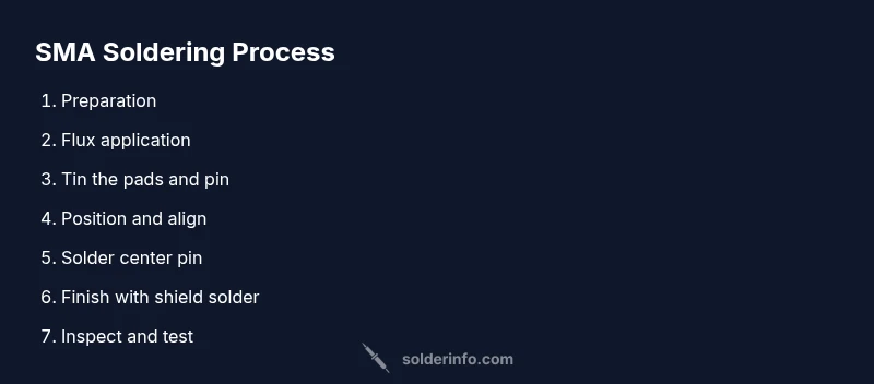
- 1
Prepare workspace and safety checks
Set up a clean, well-lit, ESD-safe area. Put on an anti-static wrist strap and goggles. Gather all tools and materials, then inspect the SMA footprint on the PCB for alignment with the connector’s ground lugs.
Tip: Clamp the PCB to a stable surface to prevent movement during soldering. - 2
Choose the correct SMA connector and footprint
Verify the connector type (PCB mount vs SMT) and footprint. Check the center pin orientation and shield lug layout to ensure proper alignment with the PCB pads before touching any flux.
Tip: Double-check the footprint against the PCB design rules to avoid misfit. - 3
Apply flux to pads and connector
Lightly apply flux to the PCB pads and the connector’s mating surfaces to improve wetting and reduce surface tension during solder flow. Avoid heavy flux that can cause shorts or flux pick-up on adjacent traces.
Tip: A thin, even layer is enough; excess flux can attract dust and moisture. - 4
Tin the pads and connector center pin
Pre-tin the PCB pads and the center pin of the SMA connector with a tiny amount of solder. This helps establish a consistent starting point for the joint and makes it easier to form a proper fillet.
Tip: Keep the amount of solder modest to prevent bridging onto nearby features. - 5
Position and align the connector
Carefully align the connector so the center pin sits squarely on the pad and shield lugs sit over their respective ground pads. Use a magnifier if needed and hold steady with tweezers or a small clamp.
Tip: A jig or fixture can dramatically improve alignment for repeatable results. - 6
Solder the center pin first
Apply a tiny amount of solder to the iron tip, touch the center pin, and flow solder onto the pin only. Avoid feeding solder to the entire joint at once; quick, controlled taps help prevent heat spreading to the plastic body.
Tip: Limit dwell time on the connector body to prevent thermal damage. - 7
Solder the shield ground and verify
Solder the shield lugs to the ground pads, ensuring a continuous ground path around the connector. Inspect the fillets for uniformity and ensure no bridging with nearby traces. Use a continuity tester between the center pin and shield to confirm no short.
Tip: If needed, reflow the shield area with restrained heat to form a clean ground ring. - 8
Inspect and test the RF path
Examine the joint under magnification for even fillets and proper wetting. If available, measure the impedance path with a network analyzer or at least test with a known RF source to ensure minimal reflections and good signal integrity.
Tip: Document any deviations and adjust future footprints or process parameters accordingly.
Quick Answers
What is an SMA connector?
An SMA connector is a small RF coaxial connector designed for high-frequency signals. It provides a 50-ohm impedance path and a reliable mechanical and electrical connection when soldered properly.
An SMA is a small RF connector used for high-frequency signals and requires careful soldering for a reliable, impedance-matched joint.
Can I solder SMA connectors on a prototype PCB?
Yes, SMA connectors can be soldered on prototype PCBs, but you should ensure the footprint matches the connector and the traces around the pad remain clear of solder bridges. Use proper flux and heat control to avoid damaging the board.
Yes, but make sure the footprint fits and you control heat to avoid board damage.
What flux is best for SMA soldering?
No-clean or rosin-flux types are commonly used for SMA soldering. They wet the joint well and minimize cleanup, reducing the risk of residue affecting RF performance.
No-clean or rosin flux works well and keeps cleanup simple.
What are common signs of a bad SMA joint?
Common signs include dull or grainy surfaces, visible gaps, or a weak mechanical bond. Poor impedance control and signal reflection can also indicate a bad joint.
Dull joints, gaps, or poor signal quality signal a bad SMA joint.
Is lead-free solder suitable for RF applications?
Lead-free solder is widely used in RF work, but it can require slightly different heat control. Ensure the alloy chosen matches the application’s impedance and mechanical requirements.
Lead-free is common but needs careful heat control.
Do I need to rework if impedance changes after assembly?
If impedance changes are detected, recheck the footprint alignment, pad cleanliness, and shielding continuity. Small geometry changes can impact impedance at RF frequencies.
If impedance shifts, review the footprint and shielding, then adjust as needed.
Watch Video
Top Takeaways
- Prepare workspace and materials before starting SMA soldering.
- Align center pin and shield ground precisely for RF integrity.
- Use minimal, controlled heat and flux to prevent damage.
- Inspect joints with a magnifier and test RF performance.
- Document process changes to improve consistency over time.