BGA Reflow: A Practical Guide for Electronics Assembly
A comprehensive 2026 guide to BGA reflow, covering equipment, paste selection, reflow profiles, inspection, and troubleshooting for electronics assembly.

Definition: BGA reflow is the controlled heating process used to solder a Ball Grid Array package onto a PCB by melting solder paste beneath the pads. It relies on a precise stencil, flux, and a carefully tailored temperature profile to form reliable joints while avoiding voids and shorts. This guide covers setup, steps, and inspection for success.
What is BGA reflow?
BGA reflow is the standard method for attaching a Ball Grid Array (BGA) package to a printed circuit board (PCB). In this process, solder paste is deposited on the PCB pads via a stencil, and the BGA package is placed precisely on top. When heated in a controlled reflow environment, the solder paste melts and wets the pads, creating solder joints that roughly mimic the ball grid under the package. The outcome depends on a balance of stencil quality, flux activity, paste rheology, pad geometry, and a well-managed temperature profile. For many hobbyists and professionals, mastering bga reflow means achieving robust joints while minimizing defects such as voids, bridging, or cold joints. According to SolderInfo analysis, attention to paste quality and profile control greatly reduces rework and increases first-pass yield. The term bga reflow is widely used in electronics assembly, plumbing, and jewelry soldering, where precision is essential and time-to-operation matters.
Key factors influencing BGA reflow
Successful bga reflow hinges on multiple interacting factors. Paste choice (lead-free versus traditional alloys) affects viscosity and wetting; stencil thickness and aperture size determine paste volume under each ball; flux type and activity influence oxide cleaning and joint spread. Footprint geometry and pad design impact alignment tolerances and solder fillet formation. A well-designed reflow profile—ramp rate, soak temperatures, peak temperature, and duration above liquidus—drives consistent solder flow without excessive ball spreading or voids. Placement accuracy and board warpage are additional real-world constraints. In practice, the most common defects are voids, solder bridging, misalignment, and intermittent joints; minimizing these requires close control of paste deposition, stencil alignment, and real-time temperature monitoring. SolderInfo analysis shows that consistent stencil alignment and clean flux significantly reduce defects, especially on larger boards where thermal gradients are harder to manage.
Tools, materials, and prep work
A successful bga reflow setup starts with the right toolkit and a clean workspace. You’ll need a stencil and paste compatible with your package size, a PCB footprint matched to the BGA, flux formulated for no-clean or chosen cleaning method, and a thermally controlled reflow environment (oven or hot air station). Supporting equipment includes a microscope or magnification for inspection, ESD-safe mats and wrist straps, tweezers, lint-free wipes, and a safe waste handling plan for flux residues. Pre-reflow checks are essential: verify footprint alignment, confirm paste deposition, and inspect the BGA orientation markers. Effective pre-cleaning of pads and careful placement reduce the risk of misalignment and solder starvation during reflow. While the exact tools vary by equipment, the core principle is consistent: stable, repeatable processing under controlled heat with clean, well-prepared surfaces. SolderInfo recommends documenting your stencil thickness, paste lot, and profile settings to enable repeatability across assemblies.
Step-by-step workflow overview for BGA reflow
A typical BGA reflow workflow follows a logical sequence of preparation, deposition, placement, heating, and inspection. Start by verifying the footprint, stencil, and paste lot. Apply paste through the stencil to form consistent volumes beneath each ball. Use precise placement to position the BGA package and confirm alignment marks. Initiate a controlled preheat that removes solvents and reduces thermal shock, then ramp to the peak temperature that melts the solder paste without overheating the package. After cooling, inspect the joints for voids, tilt, or misalignment. This overview emphasizes the need for stable fixtures, predictable heat delivery, and clean materials. For practitioners, keeping records of paste type, stencil thickness, and profile parameters improves reproducibility in subsequent runs. The SolderInfo team notes that proper planning and documentation are as important as the hardware itself for achieving reliable bga reflow results.
Inspection, testing, and defect mitigation
Post-reflow inspection focuses on joint integrity, fillet shape, and the absence of major defects. X-ray or high-magnification optical inspection can reveal voids under the BGA that are not visible from the top. Common defects include voids, bridging between adjacent pads, misalignment, and non-wetting. Mitigation strategies include optimizing stencil thickness and paste volume, adjusting flux activity, and refining the reflow profile to minimize dwell time in the liquidus region. If a joint appears suspect, careful rework with a controlled heat source can reflow and reseat the package. For many assemblies, post-reflow profiling with thermocouples placed across the board helps identify hot spots and guides future process tweaks. Safety and clean-up considerations are essential: ventilate the work area and dispose of flux residues according to local regulations. SolderInfo emphasizes that systematic inspection and disciplined rework practices dramatically improve long-term reliability.
Safety, cleanliness, and best practices
BGA reflow involves high temperatures and flux fumes; proper ventilation and personal protective equipment are non-negotiable. Work in a static-free environment, and keep the workspace free of clutter to prevent misplacement of parts. Use an accurately calibrated reflow tool to minimize thermal stress on the PCB and package. Residues from flux can affect performance if not cleaned, so decide upfront whether cleaning is necessary based on flux type and product requirements. Periodically revalidate stencil integrity, check paste expiration dates, and store materials as recommended by manufacturers. The SolderInfo team recommends establishing a standard operating procedure (SOP) that covers pre-checks, deposition, placement, heating, cooling, inspection, and cleaning. By adhering to a documented process, you reduce variations and improve repeatability across production runs.
Post-reflow considerations and documentation
After the reflow cycle, a brief cooldown period helps stabilize joints. Record observations, including any anomalies and the batch ID of materials used. Maintain an ongoing log of paste lot numbers, stencil thickness, and oven profile settings to support traceability and troubleshooting. If your assembly includes sensitive components or requires conformance to a specific standard, consider an additional quality inspection or a sampling plan to validate process control over time. The SolderInfo guidance emphasizes that robust documentation supports faster root-cause analysis when defects occur and fosters continuous improvement across teams.
Tools & Materials
- BGA package and PCB footprint(Ensure footprint matches package; verify orientation marks.)
- Solder paste (no-clean or compatible)(Select alloy type per project (lead-free common). Check expiration.)
- Stencil with appropriate aperture(Apertures match pad geometry; thickness chosen for desired paste volume.)
- Flux (no-clean or post-cleaning variant)(Activity level should suit paste and stencil; use fresh flux.)
- Reflow oven or hot air rework station(Must support controlled ramp, soak, and peak temperatures.)
- Thermocouples/temperature sensors(Place to monitor preheat and peak; verify uniform board heating.)
- Microscope or high-mag inspection camera(12–20x magnification recommended for joint inspection.)
- ESD-safe workstation and PPE(Wrist strap, mat, and antistatic containers.)
- Tweezers, spatula, lint-free wipes(For precise placement and cleaning of surfaces.)
- Flux cleaner (if post-clean needed)(Isopropyl alcohol or approved solvent for residue removal.)
Steps
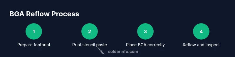
Estimated time: 60-120 minutes
- 1
Prepare footprint and stencil
Inspect the PCB footprint for pad damage, alignment marks, and solder mask openings. Verify the stencil sits flat and aligns with the pads before depositing solder paste. This reduces misalignment risk and ensures uniform paste transfer.
Tip: Align the stencil using a fiducial and verify paste coat continuity with a quick test print on a sacrificial panel. - 2
Print paste through stencil
Print a consistent paste layer onto each pad using a controlled squeegee stroke. Ensure the paste deposit volume matches the pad size to avoid excess solder or insufficient coverage.
Tip: Use a closed-door print test to verify paste height before committing to the board. - 3
Place BGA component
Carefully align the BGA package using orientation marks. Place the package straight down to avoid skew or tilt, which complicates reflow and joint formation.
Tip: Lightly hold the BGA and verify alignment under a magnifier before final seating. - 4
Preheat or ramp to soak
Begin a gentle heat ramp to remove solvents and reduce thermal shock. This step helps prevent solder starvation and component movement.
Tip: Keep the board level to avoid shifting the BGA during ramp. - 5
Execute reflow to peak
Raise temperature to the peak zone where the solder alloys melt and form joints. Maintain a short dwell above liquidus to avoid excessive ball spreading.
Tip: Avoid overheating the package; monitor real-time temps with thermocouples placed on the board. - 6
Cool and initial inspection
Cool the board under controlled conditions to prevent thermal shock. Conduct a first pass optical inspection for obvious defects such as misalignment or bridging.
Tip: Use a magnifier early to catch gross issues before cleaning. - 7
Rework if needed
If a joint is suspect, rework with controlled heat to reseat the paste, avoiding repeated cycles that can damage pads or cause delamination.
Tip: Limit rework cycles and document the change for traceability. - 8
Clean and document
Clean residues if required by flux type and file a brief run report noting paste lot, stencil thickness, and profile used. Documentation supports future process improvement.
Tip: Record any anomalies and correlate with material lots for root-cause analysis.
Quick Answers
What is BGA reflow?
BGA reflow is the controlled heating process used to solder a Ball Grid Array package onto a PCB by melting solder paste beneath the pads. It relies on a careful balance of materials, stencil precision, and a temperature profile to form solid, reliable joints.
BGA reflow is the controlled heating of a PCB to melt solder paste under a Ball Grid Array package, forming solid joints.
What equipment do I need for BGA reflow?
A stable reflow oven or hot air station, a properly engineered stencil, compatible solder paste, flux, and inspection tools are essential. A safe workspace with ESD protection completes the setup.
You need a controlled reflow oven or hot air tool, stencil, paste, flux, inspection gear, and an ESD-safe workspace.
What are common defects in BGA reflow?
Voids under the joints, bridging between pads, misalignment, and non-wetting are the most frequent issues. These stem from paste volume, alignment, and thermal profile control.
Voids, bridging, misalignment, and non-wetting are common BGA reflow defects.
Is lead-free solder required for BGA reflow?
Lead-free solder is common in many industries, but requirements vary by project. Always follow applicable standards and verify with the material data sheets.
Lead-free solder is common, but follow project standards and material data sheets.
How can I verify BGA joints without X-ray?
Use high-magnification inspection to check for bridging and tilt, and look for uniform fillets. If available, non-destructive testing like X-ray can confirm void levels.
Inspect joints with a magnifier or microscope and consider X-ray if available.
Can I perform BGA reflow without a dedicated reflow oven?
Yes, you can use a calibrated hot air station or rework station, but achieving consistent results requires careful control of heat, airflow, and profile settings. Experience and meticulous practice are key.
You can use a hot air station, but it requires careful heat control and practice.
Watch Video
Top Takeaways
- Plan the process with documentation and repeatable profiles.
- Optimize paste, stencil, and flux for reliable joints.
- Inspect joints early and after reflow to catch defects.
- Maintain a clean, ESD-safe workspace for quality results.