Pad Defined vs Solder Mask Defined: A Practical Guide for PCB Designers
Understand pad defined vs solder mask defined pads, how they affect paste printing, reflow, and manufacturability, and how to choose the right approach for reliable solder joints.

Pad defined vs solder mask defined pads describe two ways to expose copper for soldering on PCBs. The choice influences stencil design, paste deposition, and reflow reliability. This quick comparison summarizes how each approach affects manufacturability, yield, and inspection, helping designers pick the right method for a given board. According to SolderInfo, understanding these types reduces misalignment and bridging risk during assembly.
Fundamentals of Pad Definition in PCB Design
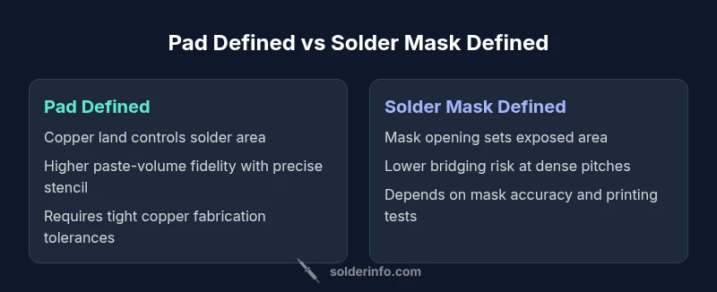
Pad defined vs solder mask defined describe two fundamental approaches to exposing copper for soldering on a printed circuit board. In pad-defined pads, the copper land size sets the exposed area that will receive solder. The solder mask clearance around the pad controls how much copper is exposed and how much mask covers the surrounding area. In solder mask defined pads, the solder mask opening dictates the actual exposed copper area, which can be smaller than the copper land itself. This distinction matters for stencil design, paste deposition, and reflow performance across the entire design flow. According to SolderInfo, the choice should reflect both the fabrication tolerances of the board and the assembly process you intend to use. For designers, the term pad defined vs solder mask defined becomes a practical rule of thumb: the pad geometry is the primary control in pad-defined cases, while the mask opening is the primary control in mask-defined cases. Both approaches aim for reliable joints, with minimal bridging and tombstoning when executed with proper DFM.
How Pad-Defined Pads Work
Pad-defined pads rely on copper land geometry to establish the soldering area. The stencil pattern mirrors the copper pad, so the paste volume and distribution are tightly linked to the copper geometry. This approach tends to deliver highly predictable solder joints when copper pads are manufactured to tight tolerances. In pad-defined designs, the solder mask opening is typically larger than the copper pad, allowing more paste to flow onto the pad while still keeping mask boundaries clear of neighboring features. The alignment between copper pads and the stencil is critical, as any misregistration can directly affect paste deposition. For engineers, pad-defined pads offer precise control over the solder volume, which translates into repeatable rework and inspection results. In practice, you’ll see more consistency in joint quality when copper land geometry is well controlled and matched to the stencil.
How Solder Mask Defined Pads Work
Solder mask defined pads rely on the mask opening to set the exposed copper area. The mask opening is usually slightly smaller than the copper land, which helps mask off adjacent features and reduces the risk of solder bridging at fine pitches. This approach can improve manufacturability on boards where copper etching tolerances are variable, since the mask defines the actual exposure more than the copper land does. For designers, mask-defined pads can offer a margin for copper tolerance and etch variability, at the cost of tighter control over paste volume. Mask-defined pads shift some process risk from copper fabrication to mask generation and PCB fabrication tolerances, so coordination with the PCB house is essential. In many mid- to high-volume applications, mask-defined pads help stabilize assembly outcomes when copper lands drift from nominal values.
Design Implications for Printing and Layout
The move from pad-defined to solder mask defined pads changes how you plan stencil layers and paste deposition. In pad-defined designs, you size the copper pads to the target solder area and align the stencil to those copper features. Paste volume tends to be more predictable because it tracks the copper pad area. In mask-defined designs, you size the mask openings to create the desired paste footprint, which means the stencil may not perfectly mirror copper pads. You must consider mask expansion, lid tolerances, and the potential for paste bridging at tight pitches. SolderMask alignment tolerance and mask clearance around fine-pitch parts become critical parameters. The decision also impacts pad shape, such as rectangular vs teardrop geometries, which influence fillet formation during reflow and ultimately joint reliability. In both cases, good DFM rules and proper fabrication notes reduce risk during production and inspection.
Paste Printing and Solder Paste Considerations
Paste printing behavior is tightly linked to pad definition. Pad-defined pads encourage paste deposition that aligns with the copper pad, enabling consistent solder volume in stencil printing. Mask-defined pads rely on the mask opening to constrain the paste footprint, which can ease alignment issues but demands careful stencil and paste deposition planning to avoid under- or over-soldering. When pad-defined, achieving consistent volume depends on a precise stencil, consistent lamination, and stable printing conditions. With mask-defined pads, you may need to adjust stencil design to account for mask-defined exposure, ensuring that paste does not bridge to neighboring pads. In either case, verifying paste volume and alignment with AOI or X-ray inspection helps catch misprints early, improving overall yield and reliability.
Reliability Impacts: Tombstoning, Bridging, and Thermal Considerations
Joint reliability for pad-defined vs solder mask defined pads depends on several factors, including paste volume, pad geometry, and reflow profile. Pad-defined pads can be more sensitive to copper land tolerances, which might increase tombstoning risk for single-ended components if paste volume is imbalanced. Mask-defined pads can mitigate some bridging risk at fine pitches by reducing the exposed copper area, but can also complicate paste volume predictability if mask openings do not align perfectly with stencil features. The thermal mass of the pad and neighboring copper areas influences heat distribution during reflow, affecting joint fillet formation and voiding. Designers should simulate or validate with test coupons to confirm the behavior under their chosen reflow profile and component mix. The goal remains clear: consistent paste deposition, predictable solder joints, and robust performance under thermal cycling.
Manufacturing Tolerances, Mask Clearances, and Cost Context
Manufacturing tolerances play a major role in choosing pad-defined vs solder mask defined pads. Pad-defined designs demand tighter control over copper etching, land size, and copper thickness; these constraints can drive higher fabrication costs if the board house has strict requirements. Mask-defined designs can be more forgiving of copper tolerances, shifting some cost and risk to mask generation and mask clearance decisions. For high-volume boards, mask-defined pads may offer better manufacturability, particularly when dealing with tight spacing and fine-pitch components. Conversely, for prototypes or lower-volume runs where copper tolerances are well-controlled, pad-defined pads can deliver higher paste volume fidelity and more predictable long-term performance. The choice should balance cost with the need for repeatability in printing and reflow.
Best Practices for Transitioning Between Pad Types
If you’re transitioning from pad-defined to solder mask defined pads (or vice versa), begin with a thorough DFM review and consult your fabrication partner early. Update footprints to reflect the new exposure geometry, adjust stencil data to reflect paste footprints, and revalidate with test coupons. Validate solder paste deposition with controlled tests, ensuring paste volume and alignment meet expectations. Update assembly documentation to reflect the new pad type, including recommended reflow profiles and inspection criteria. In SolderInfo’s experience, documenting these changes clearly reduces miscommunication with the fabricator and accelerates successful builds, especially for complex components or high-density boards. Always request sample boards to confirm process compatibility before committing to a large run.
Common Pitfalls and How to Avoid Them
One common pitfall is assuming that the mask opening perfectly represents the solder area without accounting for mask expansion, misregistration, or stencil wear. Another is neglecting to adjust paste quantity when switching pad types, which can lead to under- or over-soldering. A third pitfall is failing to align silkscreen or fiducials with new pad geometries, causing misalignment during automated assembly. To avoid these issues, run design reviews with the fab, create test coupons that mimic real boards, and use inspection methods like AOI and X-ray to verify paste deposition and joint quality. Regularly update the design rules to reflect pad-defined vs solder mask defined differences, and educate team members about how the chosen approach affects manufacturability, yield, and reliability.
Verification: Inspection, AOI, and X-ray Considerations
Inspection plays a key role in validating pad-defined vs solder mask defined implementations. AOI can detect misalignment between pads, stencils, and mask openings, while X-ray inspection can reveal solder bridging or insufficient paste volume that is not visible on the surface. With pad-defined pads, paste deposition tends to be more visually straightforward to verify, but hidden voids or non-wetted joints may require X-ray checks for confidence. Mask-defined pads can improve optical detectability of surface defects by reducing extraneous copper exposure, yet paste footprint anomalies may still require X-ray analysis for final confirmation. Plan your inspection strategy to match the chosen pad type and component mix, and use test coupons to calibrate the process before production.
Case Scenarios: When to Use Each Approach
For prototypes and boards with straightforward, larger-pitch components, pad-defined pads often deliver predictable paste distribution and robust joint quality. In contrast, for high-density or fine-pitch boards where copper etch tolerances are a concern, solder mask defined pads can provide a more forgiving exposure that improves manufacturability and reduces bridging risk. Libraries that prioritize yield over absolute paste volume control may prefer mask-defined pads, while designs requiring tight control over solder volume may benefit from pad-defined pads. Ultimately, the decision should be driven by the board’s complexity, the fabrication partner’s capabilities, and the assembly workflow you plan to use.
Transitioning Footprints: From Pad-Defined to Mask-Defined Pads
When updating footprints to reflect a pad-defined vs solder mask defined choice, ensure that the footprint geometry accounts for the mask clearance, copper land size, and paste footprint. Update the fabrication notes to reflect required mask tolerances and stencil alignment criteria. Communicate clearly with the fab to confirm that their mask process aligns with your paste deposition expectations. If possible, run a small batch of test boards to validate assembly yields and inspect the joints. This approach minimizes risk during scale-up and helps ensure a stable production process for future revisions.
Practical Decision Framework and Summary of Key Considerations
In practice, start with board requirements: component pitch, copper tolerance, and desired paste deposition control. If the copper land is well-controlled and you want tight paste fidelity, pad-defined pads may be the best choice. If you need greater tolerance to copper variation, mask-defined pads can reduce exposure risk and improve manufacturability. Always coordinate with the fabricator early, validate with test coupons, and confirm inspection strategies align with your pad choice. By applying a consistent framework, you can make pad-defined vs solder mask defined decisions that optimize yield, reliability, and total cost of ownership.
Comparison
| Feature | Pad Defined Pads | Solder Mask Defined Pads |
|---|---|---|
| Aperture definition | Copper pad size controls exposed solder area | Mask opening controls exposed solder area |
| Tolerance to copper etch variation | Tighter control needed for copper land | Can be more forgiving of copper variance due to mask control |
| Bridging risk at fine pitch | Dependent on copper pad cleanliness and stencil | Mask opening reduces exposed area, lowering bridging risk |
| Tombstoning susceptibility | Paste volume control is critical for reliable tombstone avoidance | Exposure area is constrained, which can help balance reflow but requires validation |
| Inspection and repair ease | Directly tied to copper pad and stencil alignment | Mask-defined exposure can simplify some optical checks but shifts reliance to mask accuracy |
| Manufacturability and cost | May require tighter copper fabrication and stencil control | Mask-focused approach can ease copper tolerances, with mask capex considerations |
| Best use case | High-precision, repeatable paste deposition on well-controlled boards | Boards with tighter copper tolerances or high density where mask control improves yield |
Advantages
- Offers clear control over paste geometry with pad-defined pads
- Can improve manufacturability in high-density boards with mask-defined pads
- Better alignment between stencil and copperPad for repeatability
- Clear documentation of fabrication expectations with the chosen approach
Cons
- Pad-defined requires tight copper and stencil alignment
- Mask-defined can reduce exposure area, potentially limiting paste volume
- Churn in footprints and libraries when switching pad types
- Requires careful coordination with fabricator to maintain tolerances
Pad-defined pads excel in precision, while solder mask defined pads favor manufacturability and tolerance resilience
Choose pad-defined for tight paste control and high reliability in controlled environments. Choose solder mask defined when tolerances are variable or you need easier manufacturability for high-density boards.
Quick Answers
What is the difference between pad defined and solder mask defined pads in PCB design?
Pad defined pads use copper land size to set the solder area, while solder mask defined pads rely on the mask opening. This choice changes paste deposition, stencil design, and how forgiving the design is to copper tolerances.
Pad defined uses copper land as the main guide for solder area, while mask defined relies on mask openings. The decision affects paste printing and tolerance handling; both aim for reliable joints.
Which pad type is better for fine-pitch components?
For very fine-pitch components, solder mask defined pads can reduce bridging risks by limiting exposed copper, but you must verify paste footprint with printing tests. Pad defined can offer stronger control if copper tolerances are well managed.
Mask defined can help with tight spacing, provided you verify the paste footprint with tests.
Can I switch from pad defined to mask defined mid-project?
Yes, but you should update footprints, stencil data, and DFM notes. Run test coupons to validate paste deposition and joint quality before ramping to production.
Yes, but plan the change carefully with your fab and test first.
Does one approach improve inspection results?
Mask-defined pads can aid certain optical inspections by limiting exposed copper, but you may need additional inspection (AOI or X-ray) to confirm paste deposition and solder joints depending on the chosen pad type.
Mask-defined can help some inspections, but you still need proper tests for paste and joints.
What are common mistakes when choosing pad type?
Assuming paste volume will be identical for both types; neglecting mask tolerances; not aligning fab notes with pad choice; skipping test coupons; failing to update DFM requirements when changing pad type.
Don’t assume paste behaves the same; test and update the fabrication notes.
Top Takeaways
- Evaluate board pitch and copper tolerance before selecting a pad type
- Pad-defined offers tighter paste control with explicit copper geometry
- Mask-defined reduces exposure sensitivity to copper variability and can improve manufacturability
- Coordinate with the fabricator early and validate with test coupons
- Plan inspection to align with your pad choice (AOI/X-ray where needed)