Solder Pad Came Off: Urgent Troubleshooting Guide
Urgent troubleshooting guide for when a solder pad came off. Learn quick fixes, a diagnostic flow, and safe repair steps to restore your PCB and prevent future pad lifts.

If the solder pad came off, start with the simplest fix: reflow any remaining pad area and secure a temporary bridge to test continuity. If there's any risk of further lift, stop and inspect the PCB traces under a magnifier. This guide outlines the fastest, safe steps to restore a loose pad and prevent future damage.
Why Solder Pad Came Off Matters
When a solder pad comes away from the copper trace, the electrical connection to that node is broken. The result can be intermittent behavior, a non-working circuit, or, in worst cases, a short if a nearby copper plane spans the removed area. A lifted pad also increases susceptibility to contaminants and mechanical stress from handling. For hobbyists and professionals alike, recognizing that a pad has detached early is crucial: it guides you to the least destructive repair path and helps protect adjacent traces from heat and mechanical damage. In many electronics projects, the pad is the first barrier between the component and the board; once it’s gone, everything downstream becomes unreliable. Solderpad detachment typically stems from heat exposure, over-torqued connections, or aging solder joints, so your approach must prioritize controlled warming and careful reattachment to preserve copper integrity.
Immediate Risks and Why You Should Fix It Now
A missing pad creates a risk of open circuits, intermittent connections, or shorts if the exposed trace touches nearby copper. Prolonged operation without repair can erode signal integrity, create unpredictable behavior, or cause cascading failures in more complex assemblies. The sooner you address a soder-pad issue, the higher the chance you’ll avoid more extensive damage and costly repairs later. Prioritize a controlled soldering environment, avoid excessive heat cycles, and minimize mechanical strain on the board while you work. Even if you think the problem is minor, treating it promptly reduces the likelihood of trace lifting or pad delamination during testing and use.
Common Causes and How to Avoid Them
Pad lift is often caused by excessive heat during soldering, poor pad adhesion, or mechanical stress from bending or flexing the PCB. Flux depletion and contaminated pads can also weaken joints, making lift more likely on subsequent rework. To reduce risk, use the right temperature profile for the solder alloy, ensure fresh flux, and keep boards flat during soldering. For SMD pads, avoid leaning the iron on the pad and keep the tip clean to prevent unintended extra heat in adjacent regions. When possible, switch to gentler preheating and shorter contact times to protect both pad and trace.
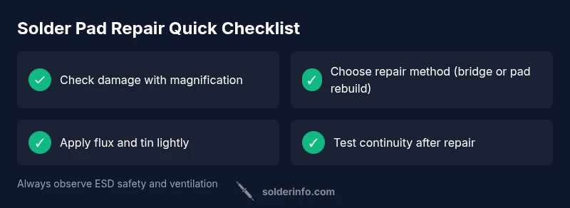
Diagnostic Checklist: Quick Visual Tests
- Inspect with a good magnifier or microscope for residual copper, lifted copper islands, or torn pads.
- Look for solder bridges connecting adjacent pads; they can masquerade as a good joint while still leaving the pad nonfunctional.
- Check trace continuity with a multimeter on resistance mode; a broken path will show high resistance or open circuit.
- Surface contamination or flux residue can masked issues; clean the area with isopropyl alcohol and re-check.
- If a pad is missing, assess whether the trace still ends in a lands pattern or if it’s lifted from the pad site; this guides the repair path.
Step-by-Step: Reattachment with Flux and Solder Bridge
- Prepare the area: power down, discharge any residual energy, and set up a clean, well-lit workspace.
- Apply a small amount of flux to the current pad area and the exposed trace end to promote wetting.
- Tin the exposed copper lightly with fresh solder so you have a tiny fillet ready for a bridge.
- Place a thin wire or copper foil bridge across the gap, aligning to avoid shorts with neighboring pads.
- Reflow the joint with a fine-tipped iron, establishing a smooth fillet that does not wick into adjacent pads.
- Inspect under magnification for proper wetting and confirm there are no bridges to nearby copper; trim any excess bridge material.
- Test continuity with a multimeter; the pad should be connected to the intended node with low resistance.
Step-by-Step: Pad Reconstruction When Pad is Missing
- If the original pad is absent, determine if you can reconstitute the pad with a copper trace extension using fine copper foil or a very thin wire.
- Solder the edge of the foil or wire to the nearby trace and route it toward the component lead, keeping it short and avoiding age; secure with a tiny dab of adhesive if needed to prevent movement.
- Tin the surface to create a new land area that can receive the component lead or a test probe when checking continuity.
- Reflow carefully to avoid creating any shorts to nearby pads; verify geometry with a magnifier and adjust as required.
- Re-test the circuit with a meter to ensure proper connectivity; inspect for cold joints or voids.
Tools, Materials, and Safe Work Practices
- Fine-tip soldering iron, temperature-controlled if possible
- Solder flux and rosin-core solder suited to electronics
- Solder wick (desoldering braid) for cleanup and leveling
- Magnification device (loupe or microscope) for precision work
- Fine wire or copper foil for pad reconstruction when needed
- Isopropyl alcohol, lint-free wipes for cleaning residue
- ESD protection such as a wrist strap and grounded work surface
- Ventilation or fume extractor to manage flux fumes
Prevention: How to Reduce Future Pad Lift
- Use proper heat management: avoid overheating the PCB and components; use a temperature-controlled iron and a suitable preheat when needed.
- Apply flux sparingly but consistently to improve wetting and reduce heat required to form a good joint.
- Inspect pads before rework; replace damaged pads or traces rather than forcing a fix that may fail later.
- Use mechanical protection: support the board during soldering to prevent flexing.
- After repair, clean flux residue and perform functional tests in multiple orientations to catch latent issues early.
Steps
Estimated time: 60-120 minutes
- 1
Power down and prep workspace
Shut off power, disconnect any batteries, and discharge capacitors as needed. Set up a clean bench with proper lighting and an ESD-safe mat. Gather your tools and verify you have a magnifier handy.
Tip: Use an anti-static mat and wrist strap to prevent damage to sensitive parts. - 2
Inspect damage under magnification
Carefully examine the pad, trace end, and neighboring copper for lifted copper, torn land, or contamination. Assess whether the trace is intact enough to accept a bridge or if a pad reconstitution is needed.
Tip: Document the damage with a photo to guide repair and for future reference. - 3
Decide repair method
Choose between a small bridge repair, pad reconstruction, or full pad replacement based on the observed damage. Simpler fixes are less risky but may not be permanent; complex damage may require rework or PCB replacement.
Tip: If the trace looks damaged, plan to reconstitute the pad rather than reusing a damaged land. - 4
Apply flux and tin the area
Apply a small amount of flux to the exposed copper and lightly tin the area to improve wetting. Do not flood the area with flux; you want a precise, controlled joint.
Tip: Flux improves heat transfer and prevents oxidation during soldering. - 5
Create a bridge or new land
Use a thin wire or copper foil to bridge to the component lead or to reconstruct the pad land. Ensure a clean path that doesn’t bridge to adjacent pads.
Tip: Trim any excess bridging material to avoid shorting neighboring pins. - 6
Reflow and inspect
Reflow the joint with a steady, controlled motion. Inspect the joint under magnification for proper wetting and no unintended bridges. If needed, rework until the joint is smooth and secure.
Tip: Avoid prolonged heat; if needed, cool the area between passes to prevent damage. - 7
Test connectivity
With power off, use a multimeter to verify continuity from the pad to the intended node. Confirm there are no shorts to adjacent pads or copper planes.
Tip: Test in multiple orientations if the device will operate in various positions. - 8
Finalize and clean
Clean flux residue with isopropyl alcohol and inspect for cleanliness. Reinstall the component and perform functional testing in-circuit to ensure proper operation.
Tip: Store repair photos and notes for future reference; consider a post-repair inspection after several cycles of use.
Diagnosis: Pad visibly lifted or no connectivity at a specific node
Possible Causes
- highExcessive heat during soldering
- mediumMechanical stress or flexing of the board
- lowOld or damaged copper trace
- lowInsufficient flux or poor pad design
Fixes
- easyReflow pad with a fine-tip iron and add a small bridge or reconstitute pad with copper foil
- mediumReconstruct missing pad with copper foil or fine wire if trace is intact
- hardReplace PCB section or whole board if traces are extensively damaged
Quick Answers
What should I do first if a solder pad has come off?
Power down the device, inspect the area under magnification, and verify whether the pad or trace is damaged. Decide on a repair path (bridge or reconstruction) before applying heat. Gentle, controlled heat preserves copper and avoids further lift.
Power down and inspect the area under magnification, then choose a repair path that avoids further damage.
Can I fix a lifted pad on a small PCB at home?
Yes for many small pads with careful reflow or pad reconstruction. If the trace is severely damaged or multiple pads lift, professional repair or board replacement may be necessary.
Yes, with care, you can fix many pads at home, but assess trace damage first.
Is it safe to use copper foil to reconstruct a missing pad?
Copper foil or fine wire can work to recreate a pad, provided the bridge is precise and there’s no risk of shorting neighboring pads. Tin the foil and align accurately before soldering.
Copper foil can work if you align it precisely and avoid shorts.
What tools are essential for repair?
You’ll need a fine-tipped soldering iron, flux, solder, desolder wick, magnification, and ESD protection. A heat sink or chip holder can help control heat during critical joints.
A fine tip iron, flux, solder, wick, magnification, and ESD gear are essential.
When should I replace the PCB instead of repairing?
If there are widespread pad lifts, extensive trace damage, or multiple failed joints, replacement or board-level repair may be more reliable than a risky single-pad repair.
If damage is widespread or complex, replacement is often the safer option.
Watch Video
Top Takeaways
- Identify pad lift early to prevent further damage
- Choose repair method based on damage scope
- Use controlled heat and proper flux for reliable joints
- Test continuity and function after repair