Burnt Solder Pad: Diagnosis and Repair Guide
Urgent guide to identify, diagnose, and repair burnt solder pads on PCBs. Learn causes, step-by-step repair with copper foil, and best practices to prevent recurrence.

A burnt solder pad is typically caused by overheating or poor heat sinking, leading to pad lift or copper delamination. Start by stopping heat, inspecting visually, and testing continuity. Then choose a repair path—patch with copper foil for minor damage or replace the pad entirely if the copper is lifted or traces are compromised.
What qualifies as a burnt solder pad?
A burnt solder pad occurs when the copper pad on a PCB overheats during soldering or desoldering, causing damage such as lifted copper, lifted traces, or oxide buildup that prevents reliable solder joints. The result can be intermittent connections, increased resistance, or open circuits. In many hobby and professional repairs, burnt pads are a leading source of recurring failures, especially on fine-pitch components where heat spreads quickly. According to SolderInfo, recognizing the signs early can save a board from irreversible damage: darkened copper, visible lift at the pad edge, and solder joints that crack or crumble under inspection. This is not just a surface issue—if the copper foil has peeled away or the substrate shows dark charring, the repair becomes more complex. In the following sections, we break down causes, immediate actions, and long-term repair strategies so you can regain reliability without risking shorts or further pad damage.
Why burnt solder pads happen and how heat plays a role
Overheating is the primary culprit. When the iron tip stays in contact too long or the heat is too high for the pad material, copper can soften, lift, or even burn the solder mask. Inconsistent heating leads to uneven joints, while poor heat sinking on a dense board prevents the pad from reaching the correct temperature. Accumulated flux residues and oxidation also raise resistance, increasing the likelihood of a cold joint when you attempt to reflow. High-frequency or high-current traces are especially vulnerable because rapid thermal cycling stresses the copper and substrate. Proper temperature control, good heat sinking, and appropriate tip selection are essential precautions that reduce the risk of a burnt solder pad.
Practical signs to look for during inspection
- Darkened or dull copper around the pad
- Edges that appear lifted or separated from the board
- Residual flux or solder splashes bridging adjacent pads
- A joint that wobbles or decouples when probed
- Physical charring or damage to the solder mask around the pad
Use a magnifying glass or microscope for precise assessment. If you observe lifted copper extending beyond the pad or cracked traces, you may be dealing with pad or trace damage that requires patching rather than simple reflow.
Immediate steps you should take when you notice damage
- Stop applying heat and disconnect power to the board to avoid shorts. 2) Visually inspect the pad under good lighting; note whether the pad is lifted, the copper is peeled, or the trace is damaged. 3) Clean flux residues with isopropyl alcohol and a soft brush; residue can obscure the true condition. 4) Continuity-check the pad and its trace with a multimeter; if there is any open circuit, plan a repair path that restores connectivity. 5) Decide whether to repair the pad in place, patch with copper foil, or replace the pad/PCB region. If the board carries critical functionality or trace integrity is compromised, consider professional help.
Repair strategies: from mild damage to pad lift
For minor damage, you can often re-tin the pad and reestablish a reliable solder surface. For lifted pads or delaminated traces, patching with copper foil or copper tape is usually required. In severe cases where the pad or trace cannot be repaired in situ, you may need to enlarge copper islands and reconnect via jumpers, or replace the PCB section. The choice depends on pad size, trace width, and circuit importance. Always verify the repaired area with a multimeter and, if feasible, reflow to test mechanical and electrical reliability.
Tools and materials you’ll want on hand
- Fine-tipped soldering iron with temperature control
- Desoldering wick (solder braid) and flux
- Copper foil or copper tape (pre-tinned if possible)
- Solder (lead-free preferred for safety, Sn96.5/Ag3/Cu0.5 typical core) and flux pen
- Magnification aid (loupe or microscope)
- Isopropyl alcohol and lint-free wipes
- Copper scrub pad or fiberglass pen for surface prep
- Kapton tape for masking and heat protection
- Multimeter for continuity checks
Gather these before starting repairs to minimize heat exposure and reduce the risk of collateral damage.
Step-by-step rework: pad repair with copper foil
- Safety and prep: power down, wear safety glasses, and set the iron to a moderate temperature with a fine tip. Deglaze the pad by gently removing old solder and flux with braid. 2) Clean the area: scrub the pad and adjacent copper to reveal fresh metal. 3) Cut copper foil patch: ensure patch size covers the damaged pad plus a margin for reliable adhesion. 4) Secure the patch: align the foil over the pad and anchor with a small dab of flux. 5) Solder patch edges: apply light, controlled solder along the foil edges to form a solid bond without shorting nearby pads. 6) Check the patch: inspect for bridging, ensure pad lands are clean, and rework as needed. 7) Reflow or re-tin: reflow the pad area or tin the patch to prepare for the final component soldering. 8) Test connections: again verify continuity and, if possible, functional behavior with the circuit powered at a safe level.
Soldering best practices to prevent future damage
- Use heat sinks or hold-down tools to minimize heat diffusion into surrounding copper and traces. - Choose the right tip size: a fine tip for small pads and a larger one for larger areas. - Apply a small amount of flux and ensure the pad is clean before tinning. - Avoid excessive heating time; work in short bursts and test after each step. - Inspect for residue after soldering and clean thoroughly to prevent future shorts.
Safety and failed repair indicators
Always observe safety: unplug the board, avoid inhaling fumes, and work in a well-ventilated area. If you observe scorching, melted solder mask, or persistent open circuits after repair attempts, stop and seek professional help. Do not risk further damage by forcing additional patches on fragile pads; consider a PCB rework service or replacement if the board is valuable.
Preventive practices to extend board life
Adopt heat-managed soldering protocols: set a suitable temperature, short contact times, and adequate cooling between joints. Maintain clean surfaces and avoid reuse of damaged pads. For frequent repairs, consider pre-applied copper shields or redesigned pads for easier maintenance.
Steps
Estimated time: 60-90 minutes
- 1
Power down and prep
Disconnect power and remove any energized circuits from the board. Put on eye protection and set up a clean workspace with good lighting. Inspect the area for obvious damage before starting.
Tip: A well-lit, static-safe workspace reduces accidental damage. - 2
Assess pad damage
Use a magnifier to inspect the pad, adjacent traces, and solder mask. Decide whether you can rework in place or if patching is required.
Tip: Document the damaged area with a photo for reference. - 3
Prepare surface
Clean the pad and surrounding copper with isopropyl alcohol. Remove old flux and solder residues so fresh solder adheres properly.
Tip: Avoid harsh abrasives that can further lift copper. - 4
Patch with copper foil
Cut a patch larger than the damaged pad, align it, and secure with flux. Solder the edges carefully to form a solid connection without bridging nearby pads.
Tip: Keep flux thin and move slowly to avoid thermal shock. - 5
Re-tin and test
Tin the repaired area and perform a continuity check with a multimeter. Verify adjacent pads and the patched region are electrically sound.
Tip: Test at low voltage first to prevent component damage. - 6
Reassemble and monitor
Reconnect power, boot the device, and monitor for proper operation. If any signs of failure reappear, reassess or replace the affected PCB region.
Tip: If in doubt, pause and consult a professional.
Diagnosis: Board shows a burnt pad after attempting soldering or desoldering
Possible Causes
- highOverheating due to prolonged contact or high iron temperature
- mediumPad lift from mechanical stress or substrate delamination
- mediumInadequate heat sinking or insufficient flux
- lowContamination or flux residue causing poor adhesion
Fixes
- easyReduce iron temperature and limit contact time; use a heat sink for the pad
- mediumIf pad is lifted, patch with copper foil or tape and re-establish a conductive trace
- easyClean area thoroughly and apply fresh flux; reflow with careful temperature control
- hardIf copper traces are damaged, replace the section or seek professional PCB repair
Quick Answers
What causes a solder pad to burn?
Burns are typically caused by excessive heat, prolonged contact with the iron, or poor heat sinking. Contaminants and aging PCB material can worsen the effect, leading to pad lift or delamination.
Burns usually come from too much heat or not enough heat sinking during soldering.
Can I repair a burnt pad without replacing the PCB?
In many cases you can repair with a copper patch or foil if the damage is local. If the copper is lifted or the trace is broken, patching or re-routing may be needed. Severely damaged areas might require PCB replacement.
Most fixes involve patching or re-routing, not replacing the entire PCB.
What tools are essential for repairing burnt pads?
A fine-tipped temperature-controlled iron, desoldering wick, copper foil or tape, flux, magnification tool, and a multimeter for continuity checks are essential.
You’ll want a fine iron, flux, copper patch materials, and a tester.
How can I prevent burnt pads in future projects?
Use appropriate heat settings, practice proper tinning techniques, ensure good heat sinking, and keep pads clean. Plan joints to minimize heating time and inspect pads after initial reflow.
Choose the right heat, sink the pad, and keep joints clean to prevent future issues.
When should I seek professional PCB repair?
If the pad lift is extensive, traces are damaged, or the board is high-value, professional repair services can avoid further damage and preserve board functionality.
If the damage is big or critical, consider a professional repair.
Is hot air rework safer than a soldering iron for pads?
Hot air can provide more uniform heating for complex pads, but it requires careful control to avoid lifting adjacent traces. For small pads, a precision iron with a fine tip is often safer.
Hot air can be useful but needs careful control; for tiny pads, a fine iron is usually best.
Watch Video
Top Takeaways
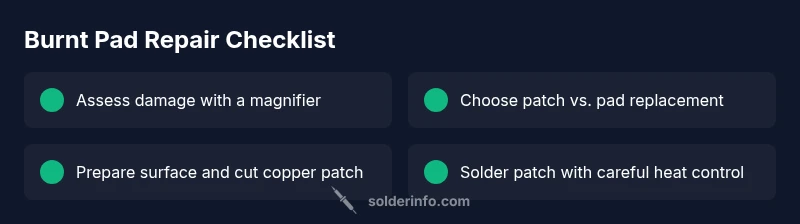
- Assess pad damage before attempting repair
- Use copper foil patches for lifted pads
- Control heat with proper tools and techniques
- Test continuity after each repair step
- If uncertain, seek professional PCB repair