Solder Mask vs Nail Polish: A Practical Comparison for Soldering
A thorough, expert comparison of solder mask and nail polish for electronics. Learn about insulation, heat resistance, application, removal, and when each option is appropriate for hobbyists and professionals.

What the comparison means for electronics projects
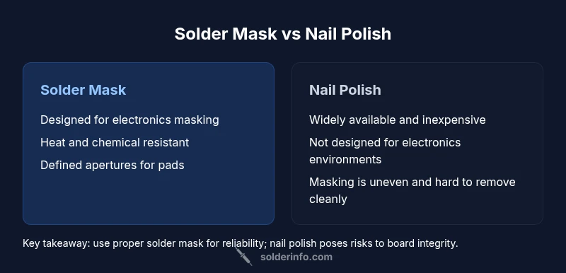
Broadly, solder mask is a specialized layer used to insulate copper traces on PCBs, control copper exposure, and withstand soldering heat. Nail polish, a cosmetic coating, is not manufactured for electronics and lacks defined apertures. The distinction matters because a masking material directly influences electrical performance, heat management, reliability, and rework options. According to SolderInfo, many hobbyists try nail polish as a quick hack, but this approach introduces unpredictable results and safety concerns. For this reason, the solder mask vs nail polish debate is not simply about aesthetics; it is about meeting standards for insulation, cleanliness, and durable solder joints.
In practical terms, you should evaluate how the masking layer will behave under soldering temperatures, during cleaning, and across rework cycles. Solder mask is engineered to tolerate fluxes and solvents often used in rework, whereas nail polish can soften, crack, or peel when exposed to heat or harsh chemicals. The SolderInfo team emphasizes that the best outcomes come from materials designed for electronics, even if the initial cost or learning curve is higher. This first block sets the stage for a deeper dive into the material science and process implications of each option.
bold:1]
Material and thermal properties: how heat and chemicals affect masking options
A crucial differentiator between solder mask and nail polish is their performance under heat and chemical exposure. Solder mask is formulated to withstand typical soldering environments, resist fluxes, and maintain adhesion during heating cycles. Nail polish, especially cheaper formulations, can soften, melt, or debond from copper surfaces when exposed to soldering heat or aggressive solvents used in flux removal. Over time, softened coatings can trap moisture or encourage corrosion at pad edges. From the perspective of reliability, mask material selection influences joint quality, pad geometry, and the risk of unwanted copper exposure. The SolderInfo analysis suggests that even small margins of error in coverage can cause bridging or cold joints if masking fails during rework. For most electronics work, this makes solder mask the safer, more predictable choice.
Coverage control and aperture definition: Why precise masking matters
One of the primary advantages of true solder mask is its ability to create well-defined openings for pads and vias, while covering the rest of the copper traces to prevent unintended solder wicking. Nail polish lacks consistent mask thickness and may blur edges, leading to inconsistent solder fillets or accidental shorts. In high-density boards, precise apertures are essential to preserve signal integrity and heat dissipation pathways. The ability to reproduce identical patterns across multiple boards is another key advantage of solder mask, ensuring repeatable manufacturing results. Hobbyists who attempt nail polish often encounter irregular borderlines that complicate inspection and automated optical recognition in production settings.
Application methods and practicality: industrial masks vs DIY coatings
Solder mask is typically applied through a controlled process in PCB fabrication houses or through specialized mask painting and curing systems in professional shops. It includes a defined cure schedule, controlled thickness, and predictable adhesion to the copper surface. Nail polish, by contrast, is a consumer product designed for nails, not electronics. Its application is manual and variable, with differences in brush consistency, layer thickness, and curing behavior under ambient conditions. For hobbyists, nail polish may seem convenient, but achieving uniform coverage over irregular board shapes is challenging. The result can be inconsistent masking and a higher likelihood of accidental contact with solder joints during assembly. The practical takeaway is that the reliability of a masking layer in electronics is closely tied to the quality and compatibility of the application process.
Durability, wear, and rework potential
Mask durability is a core consideration for long-term reliability. Solder mask is designed to resist solvents, fluxes, and mild abrasion during cleaning and rework, maintaining protective coverage over the board through multiple thermal cycles. Nail polish can crack, chip, or flake with handling or cleaning that involves acetone or isopropyl alcohol, exposing copper and risking corrosion or oxidation. Rework is more straightforward with solder mask because the mask is compatible with standard repair techniques and can be reapplied. Nail polish often requires aggressive removal methods that may damage the copper traces or pads. The durability trade-off here is clear: for critical electronics, solder mask provides superior reliability and easier maintenance.
Removal and rework considerations
Removing solder mask requires solvents or controlled thermal exposure in a way that minimizes damage to copper traces. Rework often involves removing a layer, cleaning the surface, and reapplying new mask. Nail polish removal is frequently more aggressive and may leave residue or cause micro-scratches on copper surfaces, complicating subsequent soldering. In many hobby contexts, people attempt to peel off nail polish with household solvents, only to discover residual film and pad oxidation that compromise solder joints. From a process perspective, the ability to cleanly remove masking without harming the board is an indicator of a masking option’s suitability for iterative prototyping and frequent changes.
Safety, chemicals, and environmental impact
Coatings used in electronics are selected not only for performance but for safety. Solder mask formulations are designed to minimize hazardous fumes and provide robust environmental resistance. Nail polish products contain dyes and solvents that may emit stronger fumes or leave residues. Handling solvents for nail polish can pose skin and respiratory hazards, particularly in small, poorly ventilated spaces. The environmental impact of disposal is also a factor; many electronics shops have guidelines for masking material waste. The overall safety profile strongly favors proper solder mask materials over cosmetic polishes when the masking task is embedded in a formal electronics workflow.
Cost, accessibility, and value considerations
Cost is a major practical factor. Solder mask is an industry-standard material with a cost that reflects its engineering purpose and manufacturing context. Nail polish, while inexpensive per bottle, becomes less economical when considering the need for repeated rework, cleanup, and the risk of board damage. Accessibility also differs: solder mask is typically available through PCB fabrication services and electronics supply channels, whereas nail polish is ubiquitous in consumer stores. For hobbyists and professionals alike, the value proposition hinges on how much you value reliability, repeatability, and board longevity versus upfront convenience and low initial cost.
Practical recommendations for hobbyists and professionals
For hobbyists engaging in occasional prototyping, nail polish might seem tempting for speed, but it is best treated as a temporary masking approach with clear limitations. For any project intended for extended use, or where performance matters, invest in proper solder mask materials and a controlled masking process. Using Kapton tape or liquid masking products designed for electronics can offer a middle ground for temporary masking without compromising the board’s integrity. Professionals should adopt mask materials that align with their rework schedules, cleaning protocols, and thermal profiles. The bottom line is to align masking choice with project requirements rather than convenience alone.
Decision framework: when to choose each option
In deciding between solder mask and nail polish, start with the project’s density, heat exposure, and required reliability. If the board features high-density traces or requires repeated soldering and rework, choose solder mask. For ultra-fast, low-stakes prototyping where inspection can tolerate visible traces and mask borders, a nail-polish approach could be considered, with the understanding of its drawbacks. Always test on a sacrificial board to validate adhesion, thermal tolerance, and cleanup before committing to production. Finally, document your masking approach for future maintenance and reproducibility.
Alternative masking options for prototyping and quick-turn work
Beyond traditional solder mask, other masking options can support rapid prototyping. Temporary masks like low-tack Kapton tape or specialized liquid masking products exist to cover copper while exposing pads. Painter’s tape can be used for simple, low-density boards but is prone to gaps and edge lift. Conformal coatings designed for electronics provide another layer of protection, although they require curing time and specialized solvents for removal. The best practice is to choose masking methods that match your tolerance for risk, time, and rework needs, and to validate through small-test boards before scaling up.
Authority sources and further reading
To corroborate the safety and reliability considerations discussed here, consult authoritative sources such as OSHA guidelines for chemical handling, NIST standards on material properties, and IEEE articles on PCB masking practices. These resources provide foundational information about how masking materials interact with heat, solvents, and copper traces, helping you make informed decisions for both hobby projects and professional work. For practical steps and tested methods, see the linked references and ensure you reference official guidance in your workflow.