Wave Solder vs Dip Solder: A Practical Comparison for Electronics Soldering
Compare wave soldering and dip soldering for electronics projects. Learn differences, throughput, board compatibility, and best practices for through-hole and mixed-density designs.

Wave solder vs dip solder: both methods apply molten solder to joints, but they fit different board designs and production scales. Wave soldering delivers high throughput for through-hole assemblies and large volumes, while dip soldering provides greater control for mixed-density boards and prototyping. The best choice hinges on board design, volume, and cost constraints.
What wave soldering and dip soldering are
Wave soldering and dip soldering are two long-standing methods used to join components to PCB assemblies with molten solder. Wave soldering uses a controlled flow of solder that passes over the underside of a PCB as it travels on a conveyor, typically used for through-hole components and boards designed for high-volume production. Dip soldering involves immersing a board or a subset of joints into a solder bath, either manually or with a selective dipping fixture, allowing for precise control over individual joints, including delicate components or irregular pads.
According to SolderInfo, understanding the core mechanics of each method helps determine why one approach may outperform the other in a given factory setting. The technique you choose will influence yields, maintenance needs, energy use, and downstream processes such as cleaning and inspection. While both methods share the same physics—molten solder forming a metallurgical joint—their implementation, throughput, and suitability for different design goals diverge in meaningful ways. For hobbyists and professionals alike, a clear mental model of where each method shines is essential when planning a new build, a production line upgrade, or a capacity expansion. The keyword wave solder vs dip solder is a useful shorthand for framing the trade-offs between speed, control, and cost in electronics soldering.
Quick look at the two processes
- Wave soldering is designed for rapid deposition of solder on a moving board, typically bottom-side joints first, with controlled reflow and capture. It excels on boards with many through-hole components and consistent land patterns.
- Dip soldering is a targeted, dipping-based approach that can be manual or semi-automatic, enabling selective or full-board coverage. It offers superior control for challenging pads, heat-sensitive parts, or mixed-density assemblies. In practice, many shops use a hybrid strategy, reserving dip for problem areas and wave for the bulk.
Throughput and production scale considerations
When evaluating wave solder vs dip solder soldering, throughput is often the primary decision driver. Wave soldering can process dozens to hundreds of boards per hour depending on line speed, board complexity, and the number of through-hole joints. Dip soldering, especially in manual or selective modes, yields much slower throughput but provides precise control where components are densely packed or fragile. For high-volume manufacturing, wave soldering offers economies of scale; for small runs or prototype volumes, dip soldering minimizes setup costs and rework risk. The choice affects line layout, staffing, and maintenance cycles, all of which contribute to total cost of ownership over the life of the production equipment.
Design and board layout implications
Board design and land patterns significantly influence whether wave solder vs dip soldering is the better fit. Wave soldering benefits from uniform land patterns and consistent pad spacing, with careful consideration given to thermal profiles and wave exposure. Dip soldering tolerates more pad variability and can accommodate odd geometries, but it requires careful fixturing to avoid hotspots and cold joints. For designers, anticipating the chosen process means designing pads, vias, and neck-down features that align with the corresponding soldering method. This reduces defects and simplifies post-process cleaning.
Flux types, cleanliness, and post-solder cleaning
Flux selection plays a central role in both methods. Wave soldering typically uses fluxes formulated for robust long-contact exposure and post-wash compatibility, while dip soldering may employ fluxes tailored to selective immersion or manual dipping. Flux residue management affects inspection, cleaning, and long-term reliability. Lead-free processes, common in modern electronics, demand flux chemistries that minimize cavitation and solderability loss over time. Regardless of method, a consistent cleaning regime reduces the risk of cold joints and dendritic growth, preserving joint integrity across batches.
Lead-free and RoHS considerations
Lead-free solders introduce higher melting points and more stringent thermal control requirements. Both wave and dip soldering can accommodate lead-free alloys with appropriate fluxes and temperature profiles, but the higher heat input in wave soldering can stress heat-sensitive components if not properly managed. Dip soldering offers greater tunability for heat exposure on problematic parts, making it a pragmatic choice when boards contain temperature-sensitive components or mixed lead-free/measured solder types. In all cases, following RoHS-compliant practices and validating solder joints with inspection tools is essential.
Costs, maintenance, and energy use
Initial equipment costs, maintenance cycles, and energy consumption differ meaningfully between wave and dip soldering. Wave systems tend to require higher upfront investment and more regular maintenance (pumps, filters, and wave tanks), but they offer lower labor costs per board at scale. Dip soldering has lower capital costs and can operate with simpler fixtures or even manual setups, but it often requires more hands-on intervention for consistent results across multiple joints. Energy use correlates with temperature control, dwell time, and throughput; optimizing these factors reduces operating expenses in either method.
Process control, inspection, and quality assurance
Quality control in both methods relies on robust process control: precise temperature management, controlled dwell times, and consistent flux application. Modern systems use inline AOI (automated optical inspection) or X-ray to detect hidden defects in wave solder lines, while dip solder lines benefit from meticulous fixture calibration and visual or AOI inspection of each joint. Consistent solder joint quality hinges on stable solder bath conditions, clean boards, and well-maintained fluxing systems. Adopting a documented standard operating procedure (SOP) helps teams reproduce results across shifts and facilities.
When to choose wave vs dip: a decision framework
A practical decision framework starts with board design, production volume, and risk tolerance. If your boards have high-throughput through-hole content and standardized land patterns, wave soldering is typically the more scalable option. If you are dealing with mixed-density boards, temperature-sensitive parts, or small-volume prototyping, dip soldering offers superior control and flexibility. Consider a hybrid approach for complex assemblies, using wave soldering for the bulk of simple joints and dip soldering for problem areas or prototyping runs. The framework should also include cost of ownership, availability of skilled operators, and the ability to maintain consistent solder quality over time.
Practical tips and optimization for both methods
To optimize either method, keep lands and pads clean and well defined, minimize temperature excursions, and tune flux chemistry to the solder alloy in use. Regularly service the fluxing system, inspect solder pots for contamination, and monitor dross formation in wave tanks. For mixed-density boards, plan selective dipping zones or fixtures that minimize heat exposure to heat-sensitive components. Finally, maintain a robust training program to ensure operators understand how process parameters impact joint quality and reliability.
Real-world scenarios and case considerations
In practice, many shops manage a dual-strategy approach: using wave soldering for straightforward, high-volume through-hole assemblies and dipping techniques for prototypes, repair work, or boards with delicate or irregular patterns. One common scenario is a production line that alternates between RoHS-compliant lead-free runs and legacy lead-containing products; in this case, flux and temperature controls must be carefully calibrated to prevent cross-contamination and ensure consistent solder joints across all batches. From the perspective of the SolderInfo team, tailoring the process to the board density and component mix yields the most reliable outcomes in diverse manufacturing environments.
Summary of trade-offs and looking ahead
Understanding wave solder vs dip solder is about balancing throughput with control. Wave soldering offers speed, automation potential, and consistency for simple, high-volume through-hole boards. Dip soldering provides flexibility, precision, and better performance on mixed-density or temperature-sensitive assemblies. As manufacturing evolves, some shops adopt hybrid strategies, while others optimize either method with improved fixtures, flux chemistries, and inline inspection tools. The ongoing challenge is to align process capabilities with the specific design goals of each project and the production realities of the shop.
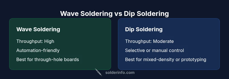
Comparison
| Feature | Wave Soldering | Dip Soldering |
|---|---|---|
| Throughput | High for through-hole, high-volume boards | Moderate to low; better for small runs |
| Process control | Automation-friendly with conveyors and tanks | Manual or selective control with fixtures |
| Initial equipment cost | Medium to high | Low to medium |
| Ideal board type | Through-hole, uniform lands, high volume | Mixed-density, temperature-sensitive parts, prototypes |
| Lead-free compatibility | Fully compatible with modern fluxes and RoHS | Compatible; requires careful control for lead-free |
| Maintenance | Regular tank/ pump maintenance; phase-out of dross | Fixture maintenance; more manual checks |
Advantages
- Highlights the trade-offs between throughput and control
- Helps plan line layout and staffing
- Assists budgeting for equipment and maintenance
- Clarifies RoHS and lead-free considerations
Cons
- Does not cover every edge case for unusual boards
- Requires design co-ordination between PCB and process
- Hybrid approaches add setup complexity
Wave soldering is preferred for high-volume through-hole production; dip soldering is best for flexibility and precision on mixed-density boards.
For large-scale, uniform boards, wave soldering offers throughput and automation benefits. For prototyping, delicate components, or irregular layouts, dip soldering provides greater control. A hybrid approach can maximize both worlds when designed thoughtfully.
Quick Answers
What are the core differences between wave soldering and dip soldering?
Wave soldering uses a continuous solder wave to cover joints as boards move; dip soldering immerses joints into a solder bath for selective or full coverage. Wave favors high-volume through-hole boards, while dip offers flexibility for mixed-density and prototyping.
Wave soldering uses a moving wave to coat joints, great for high-volume through-hole boards, while dip soldering dips joints into a solder bath for precise, flexible coverage.
Is wave soldering suitable for all PCB designs?
Not all designs suit wave soldering. Boards with dense SMT areas, fine-pitch components, or very irregular pads may require dip soldering or a hybrid approach. Plan board layout with the chosen process in mind.
Wave soldering is great for through-hole boards, but for dense or irregular designs you may need dip soldering or a hybrid setup.
Can both methods handle lead-free solders?
Yes, both methods can use lead-free solders with proper flux, temperature control, and cleaning. Ensure your flux and alloy choices align with RoHS requirements and component tolerances.
Both wave and dip soldering can use lead-free solders provided you control temperature and flux correctly.
Which method is more cost-effective for small production runs?
For small runs, dip soldering or manual dipping often costs less upfront and offers flexibility, while wave soldering incurs higher setup and equipment costs but pays off with high throughput if volumes grow.
For small runs, dip soldering is usually cheaper to start; wave soldering pays off when volumes increase.
What are common defects in wave solder and how can they be prevented?
Common defects include bridging, icicles, and cold solder joints. Prevention hinges on temperature control, proper flux application, good board cleaning, and regular maintenance of the solder bath and conveyors.
Common wave solder defects are bridged joints and cold joints; good temperature control and cleaning help prevent them.
Top Takeaways
- Assess board density to guide method choice
- Prioritize throughput for high-volume lines
- Consider component sensitivity and heat exposure
- Plan flux and cleaning for lead-free processes
- Match equipment and maintenance to production goals